

319
Compact Models for Ultrathin Body FETs
where:
f(x, y) is the electrostatic potential at any point (x, y) in the channel
q is the magnitude of the electronic charge
K si and ε 0 are the dielectric constant of the silicon channel (fin) and permittivity of free space, respectively
p(x, y), n(x, y), N x y
d
+
( )
, , and N x y
a
−
( )
, are the hole, electron, ionized donor,
and ionized acceptor concentrations at any point (x, y) of the semiconductor substrate, respectively
For a p-type substrate, the minority carrier concentration at any point (x, y) of
the substrate is given by (Equation 3.40)
n x y
n
p x
n
N
x y
v
i
i
a
k T
( , )
( )
exp
( , )
≅
=
2
2
φ
(9.6)
where:
N a is the acceptor doping concentration in a p-type substrate (assuming
complete ionization)
n i is the intrinsic carrier concentration
v kT is the thermal voltage given by kT/q
k and T are the Boltzmann constant and ambient temperature, respectively
Again, from Equation 3.35, we can show that for a p-type substrate
φ B
k T
a
i
v
N
n
=
ln
(9.7)
Gate metal
Gate metal
V gs
V gs
V ch (y)
Gate oxide
ϕ(y = 0) = ϕ s
ϕ(t fin /2,y) = ϕ s (y)
ϕ(x = 0,y) = ϕ 0 (y)
ϕ(y = L) = ϕ d
n+
Source
n+
Drain
Gate oxide
0,0
y
x
T ox
T ox
N b
t fin
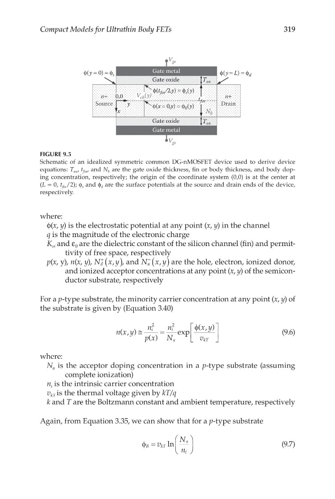
FIGURE 9.5
Schematic of an idealized symmetric common DG-nMOSFET device used to derive device
equations: T ox , t fin , and N b are the gate oxide thickness, fin or body thickness, and body doping concentration, respectively; the origin of the coordinate system (0,0) is at the center at
(L = 0, t fin /2); f s and f d are the surface potentials at the source and drain ends of the device,
respectively.
Compact Models for Ultrathin Body FETs
where:
f(x, y) is the electrostatic potential at any point (x, y) in the channel
q is the magnitude of the electronic charge
K si and ε 0 are the dielectric constant of the silicon channel (fin) and permittivity of free space, respectively
p(x, y), n(x, y), N x y
d
+
( )
, , and N x y
a
−
( )
, are the hole, electron, ionized donor,
and ionized acceptor concentrations at any point (x, y) of the semiconductor substrate, respectively
For a p-type substrate, the minority carrier concentration at any point (x, y) of
the substrate is given by (Equation 3.40)
n x y
n
p x
n
N
x y
v
i
i
a
k T
( , )
( )
exp
( , )
≅
=
2
2
φ
(9.6)
where:
N a is the acceptor doping concentration in a p-type substrate (assuming
complete ionization)
n i is the intrinsic carrier concentration
v kT is the thermal voltage given by kT/q
k and T are the Boltzmann constant and ambient temperature, respectively
Again, from Equation 3.35, we can show that for a p-type substrate
φ B
k T
a
i
v
N
n
=
ln
(9.7)
Gate metal
Gate metal
V gs
V gs
V ch (y)
Gate oxide
ϕ(y = 0) = ϕ s
ϕ(t fin /2,y) = ϕ s (y)
ϕ(x = 0,y) = ϕ 0 (y)
ϕ(y = L) = ϕ d
n+
Source
n+
Drain
Gate oxide
0,0
y
x
T ox
T ox
N b
t fin
FIGURE 9.5
Schematic of an idealized symmetric common DG-nMOSFET device used to derive device
equations: T ox , t fin , and N b are the gate oxide thickness, fin or body thickness, and body doping concentration, respectively; the origin of the coordinate system (0,0) is at the center at
(L = 0, t fin /2); f s and f d are the surface potentials at the source and drain ends of the device,
respectively.