

316
Compact Models for Integrated Circuit Design
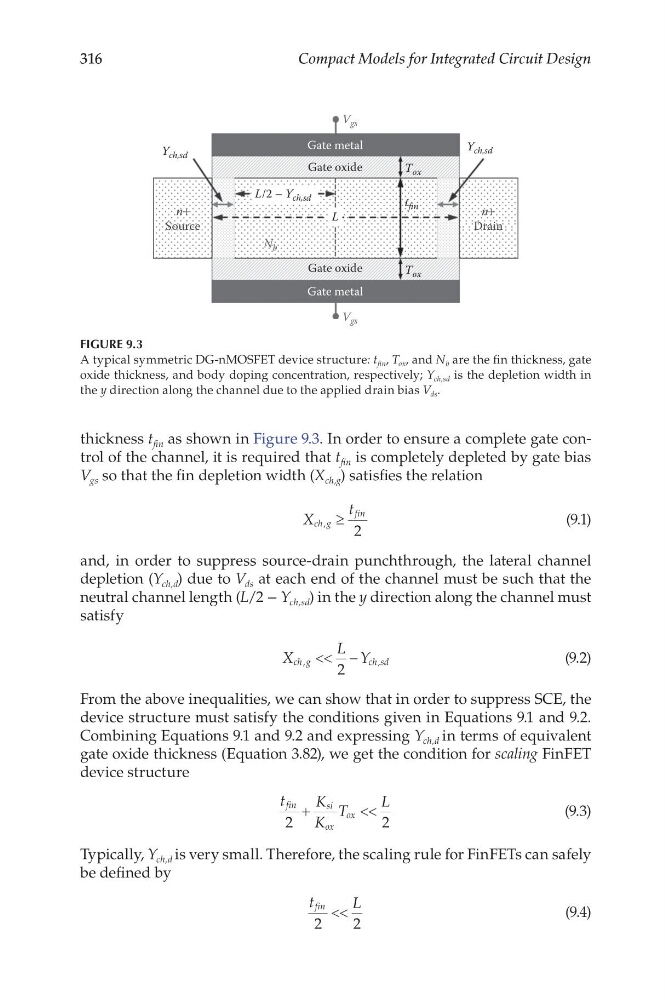
thickness t fin as shown in Figure 9.3. In order to ensure a complete gate control of the channel, it is required that t fin is completely depleted by gate bias
V gs so that the fin depletion width (X ch,g ) satisfies the relation
X
t
ch g
fin
, ≥ 2
(9.1)
and, in order to suppress source-drain punchthrough, the lateral channel
depletion (Y ch,d ) due to V ds at each end of the channel must be such that the
neutral channel length (L/2 − Y ch,sd ) in the y direction along the channel must
satisfy
X
L Y
ch g
c h sd
,
,
<< −
2
(9.2)
From the above inequalities, we can show that in order to suppress SCE, the
device structure must satisfy the conditions given in Equations 9.1 and 9.2.
Combining Equations 9.1 and 9.2 and expressing Y ch,d in terms of equivalent
gate oxide thickness (Equation 3.82), we get the condition for scaling FinFET
device structure
t
K
K
T
L
fin
si
ox
ox
2
2
+
< <
(9.3)
Typically, Y ch,d is very small. Therefore, the scaling rule for FinFETs can safely
be defined by
t
L
fin
2
2
<<
(9.4)
V gs
V gs
N b
Gate metal
Gate metal
Gate oxide
n+
Source
n+
Drain
L/2 – Y ch,sd
Y ch,sd
Gate oxide
T ox
L
T ox
t fin
Y ch,sd
FIGURE 9.3
A typical symmetric DG-nMOSFET device structure: t fin , T ox , and N b are the fin thickness, gate
oxide thickness, and body doping concentration, respectively; Y ch,sd is the depletion width in
the y direction along the channel due to the applied drain bias V ds .
Compact Models for Integrated Circuit Design
thickness t fin as shown in Figure 9.3. In order to ensure a complete gate control of the channel, it is required that t fin is completely depleted by gate bias
V gs so that the fin depletion width (X ch,g ) satisfies the relation
X
t
ch g
fin
, ≥ 2
(9.1)
and, in order to suppress source-drain punchthrough, the lateral channel
depletion (Y ch,d ) due to V ds at each end of the channel must be such that the
neutral channel length (L/2 − Y ch,sd ) in the y direction along the channel must
satisfy
X
L Y
ch g
c h sd
,
,
<< −
2
(9.2)
From the above inequalities, we can show that in order to suppress SCE, the
device structure must satisfy the conditions given in Equations 9.1 and 9.2.
Combining Equations 9.1 and 9.2 and expressing Y ch,d in terms of equivalent
gate oxide thickness (Equation 3.82), we get the condition for scaling FinFET
device structure
t
K
K
T
L
fin
si
ox
ox
2
2
+
< <
(9.3)
Typically, Y ch,d is very small. Therefore, the scaling rule for FinFETs can safely
be defined by
t
L
fin
2
2
<<
(9.4)
V gs
V gs
N b
Gate metal
Gate metal
Gate oxide
n+
Source
n+
Drain
L/2 – Y ch,sd
Y ch,sd
Gate oxide
T ox
L
T ox
t fin
Y ch,sd
FIGURE 9.3
A typical symmetric DG-nMOSFET device structure: t fin , T ox , and N b are the fin thickness, gate
oxide thickness, and body doping concentration, respectively; Y ch,sd is the depletion width in
the y direction along the channel due to the applied drain bias V ds .