

315
Compact Models for Ultrathin Body FETs
and a back gate oxide layers, a source and a drain regions, and front and
back gates. If the body is sufficiently thin, any line drawn between the source
and drain including possible leakage paths would not be far from one of the
gates. In this structure, channel doping is not required for suppressing SCEs.
Thus, RDD, a major contributor to the variation in the performance of IC
devices and VLSI circuits, is eliminated [8,9].
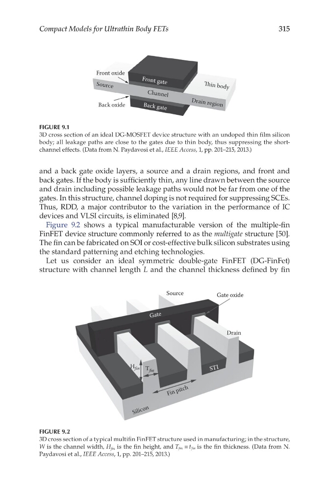
Figure 9.2 shows a typical manufacturable version of the multiple-fin
FinFET device structure commonly referred to as the multigate structure [50].
The fin can be fabricated on SOI or cost-effective bulk silicon substrates using
the standard patterning and etching technologies.
Let us consider an ideal symmetric double-gate FinFET (DG-FinFet)
structure with channel length L and the channel thickness defined by fin
Back oxide
Front oxide
So ur ce
Fr on t ga te
Ba ck ga te
Ch an ne l
Dr ain re gio n
in bo dy
FIGURE 9.1
3D cross section of an ideal DG-MOSFET device structure with an undoped thin film silicon
body; all leakage paths are close to the gates due to thin body, thus suppressing the shortchannel effects. (Data from N. Paydavosi et al., IEEE Access, 1, pp. 201–215, 2013.)
Source
H fin T fin
Gate oxide
Drain
S il ic o n
F in p it c h
G at e
ST I
FIGURE 9.2
3D cross section of a typical multifin FinFET structure used in manufacturing; in the structure,
W is the channel width, H fin is the fin height, and T
t
fin
fin
≡
is the fin thickness. (Data from N.
Paydavosi et al., IEEE Access, 1, pp. 201–215, 2013.)
Compact Models for Ultrathin Body FETs
and a back gate oxide layers, a source and a drain regions, and front and
back gates. If the body is sufficiently thin, any line drawn between the source
and drain including possible leakage paths would not be far from one of the
gates. In this structure, channel doping is not required for suppressing SCEs.
Thus, RDD, a major contributor to the variation in the performance of IC
devices and VLSI circuits, is eliminated [8,9].
Figure 9.2 shows a typical manufacturable version of the multiple-fin
FinFET device structure commonly referred to as the multigate structure [50].
The fin can be fabricated on SOI or cost-effective bulk silicon substrates using
the standard patterning and etching technologies.
Let us consider an ideal symmetric double-gate FinFET (DG-FinFet)
structure with channel length L and the channel thickness defined by fin
Back oxide
Front oxide
So ur ce
Fr on t ga te
Ba ck ga te
Ch an ne l
Dr ain re gio n
in bo dy
FIGURE 9.1
3D cross section of an ideal DG-MOSFET device structure with an undoped thin film silicon
body; all leakage paths are close to the gates due to thin body, thus suppressing the shortchannel effects. (Data from N. Paydavosi et al., IEEE Access, 1, pp. 201–215, 2013.)
Source
H fin T fin
Gate oxide
Drain
S il ic o n
F in p it c h
G at e
ST I
FIGURE 9.2
3D cross section of a typical multifin FinFET structure used in manufacturing; in the structure,
W is the channel width, H fin is the fin height, and T
t
fin
fin
≡
is the fin thickness. (Data from N.
Paydavosi et al., IEEE Access, 1, pp. 201–215, 2013.)