

310
Compact Models for Integrated Circuit Design
p-Type
buried-halos
N+DSD
N +DSD
N +SDE
N+SDE
p-Substrate
P-well
Epi
Gate oxide
nPoly/MG
Epitaxial
layer
Gate
Drain
Source
Body
p-Type V th -
adjust layer
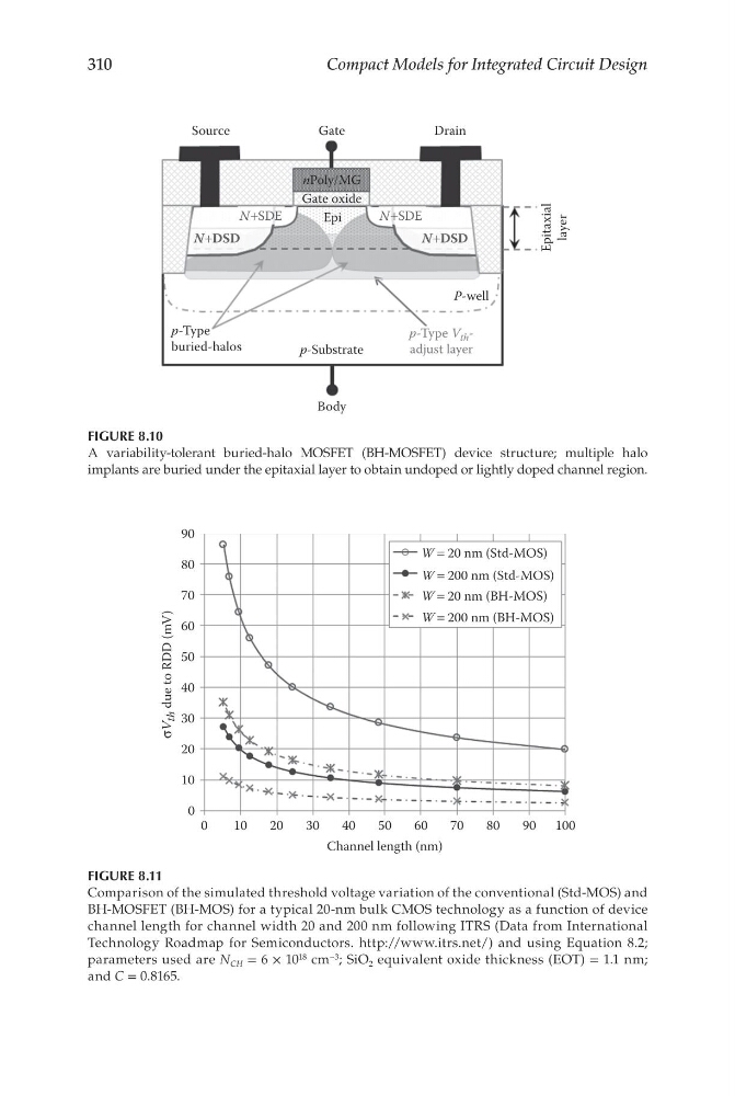
FIGURE 8.10
A variability-tolerant buried-halo MOSFET (BH-MOSFET) device structure; multiple halo
implants are buried under the epitaxial layer to obtain undoped or lightly doped channel region.
0
0
10
20
30
40
50
σV
th due to RDD (mV)
60
70
80
90
W = 20 nm (Std-MOS)
W = 200 nm (Std-MOS)
W = 20 nm (BH-MOS)
W = 200 nm (BH-MOS)
10
20
30
40
Channel length (nm)
50
60
70
80
90 100
FIGURE 8.11
Comparison of the simulated threshold voltage variation of the conventional (Std-MOS) and
BH-MOSFET (BH-MOS) for a typical 20-nm bulk CMOS technology as a function of device
channel length for channel width 20 and 200 nm following ITRS (Data from International
Technology Roadmap for Semiconductors. http://www.itrs.net/) and using Equation 8.2;
parameters used are N CH = 6 × 10 18 cm −3 ; SiO 2 equivalent oxide thickness (EOT) = 1.1 nm;
and C = 0.8165.
Compact Models for Integrated Circuit Design
p-Type
buried-halos
N+DSD
N +DSD
N +SDE
N+SDE
p-Substrate
P-well
Epi
Gate oxide
nPoly/MG
Epitaxial
layer
Gate
Drain
Source
Body
p-Type V th -
adjust layer
FIGURE 8.10
A variability-tolerant buried-halo MOSFET (BH-MOSFET) device structure; multiple halo
implants are buried under the epitaxial layer to obtain undoped or lightly doped channel region.
0
0
10
20
30
40
50
σV
th due to RDD (mV)
60
70
80
90
W = 20 nm (Std-MOS)
W = 200 nm (Std-MOS)
W = 20 nm (BH-MOS)
W = 200 nm (BH-MOS)
10
20
30
40
Channel length (nm)
50
60
70
80
90 100
FIGURE 8.11
Comparison of the simulated threshold voltage variation of the conventional (Std-MOS) and
BH-MOSFET (BH-MOS) for a typical 20-nm bulk CMOS technology as a function of device
channel length for channel width 20 and 200 nm following ITRS (Data from International
Technology Roadmap for Semiconductors. http://www.itrs.net/) and using Equation 8.2;
parameters used are N CH = 6 × 10 18 cm −3 ; SiO 2 equivalent oxide thickness (EOT) = 1.1 nm;
and C = 0.8165.