

302
Compact Models for Integrated Circuit Design
V
XW XL T U K
TH
ox
0
0 1
,
, , , ,
;
{
} where, XW and XL are the channel width and
length offset parameters due to masking and photolithography, respectively,
and account for the mismatch due to LER and LWR, whereas U0 and K1
account for the variation in µ eff and N CH under V bs , respectively. In order
to build the compact model, the variance σ ∆M mismatch is computed for each
M from a large set of data to account for the mismatch in identical paired
transistors.
8.5.2.2 Mapping Global Process Variability-Sensitive Device
Parameters to Compact Model Parameters
In Section 8.5.1.2, we have shown an analytical approach to determine the
critical set of device parameters, V W L T
R C C
th
ox
eff
D S
o v
j
0 , , , , , ,
, ,
µ γ
{
} , impacting
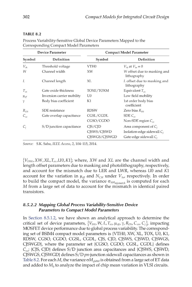
MOSFET device performance due to global process variability. The corresponding set of BSIM4 compact model parameters is {VTH0, XW, XL, TOX, U0, K1,
RDSW, CGSO, CGDO, CGSL, CGDL, CJS, CJD, CJSWS, CJSWD, CJSWGS,
CJSWGD}, where the parameter set {CGSO, CGDO, CGSL, CGDL} defines
C ov ; {CJS, CJD} defines S/D junction area capacitances and {CJSWS, CJSWD,
CJSWGS, CJSWGD} defines S/D pn-junction sidewall capacitances as shown in
Table 8.2. For each M, the variance σM global is obtained from a large set of ET data
and added to M 0 to analyze the impact of chip mean variation in VLSI circuits.
TABLE 8.2
Process Variability-Sensitive Global Device Parameters Mapped to the
Corresponding Compact Model Parameters
Device Parameter
Compact Model Parameter
Symbol
Definition
Symbol
Definition
V th
Threshold voltage
VTH0
V th at V bs = 0
W
Channel width
XW
W offset due to masking and
lithography
L
Channel length
XL
L offset due to masking and
lithography
T ox
Gate oxide thickness
TOXE/TOXM
Equivalent T ox
µ eff
Inversion carrier mobility
U0
Low field mobility
γ
Body bias coefficient
K1
1st order body bias
coefficient
R DS
SDE resistance
RDSW
Zero bias R DS
C ov
Gate overlap capacitance
CGSL/CGDL
SDE C ov
CGSO/CGDO
Non-SDE region C ov
C J
S/D junction capacitance
CJS/CJD
Area component of C J
CJSWS/CJSWD
Isolation-edge sidewall C J
CJSWGS/CJSWGD
Gate-edge sidewall C J
Source: S.K. Saha, IEEE Access, 2, 104–115, 2014.
Compact Models for Integrated Circuit Design
V
XW XL T U K
TH
ox
0
0 1
,
, , , ,
;
{
} where, XW and XL are the channel width and
length offset parameters due to masking and photolithography, respectively,
and account for the mismatch due to LER and LWR, whereas U0 and K1
account for the variation in µ eff and N CH under V bs , respectively. In order
to build the compact model, the variance σ ∆M mismatch is computed for each
M from a large set of data to account for the mismatch in identical paired
transistors.
8.5.2.2 Mapping Global Process Variability-Sensitive Device
Parameters to Compact Model Parameters
In Section 8.5.1.2, we have shown an analytical approach to determine the
critical set of device parameters, V W L T
R C C
th
ox
eff
D S
o v
j
0 , , , , , ,
, ,
µ γ
{
} , impacting
MOSFET device performance due to global process variability. The corresponding set of BSIM4 compact model parameters is {VTH0, XW, XL, TOX, U0, K1,
RDSW, CGSO, CGDO, CGSL, CGDL, CJS, CJD, CJSWS, CJSWD, CJSWGS,
CJSWGD}, where the parameter set {CGSO, CGDO, CGSL, CGDL} defines
C ov ; {CJS, CJD} defines S/D junction area capacitances and {CJSWS, CJSWD,
CJSWGS, CJSWGD} defines S/D pn-junction sidewall capacitances as shown in
Table 8.2. For each M, the variance σM global is obtained from a large set of ET data
and added to M 0 to analyze the impact of chip mean variation in VLSI circuits.
TABLE 8.2
Process Variability-Sensitive Global Device Parameters Mapped to the
Corresponding Compact Model Parameters
Device Parameter
Compact Model Parameter
Symbol
Definition
Symbol
Definition
V th
Threshold voltage
VTH0
V th at V bs = 0
W
Channel width
XW
W offset due to masking and
lithography
L
Channel length
XL
L offset due to masking and
lithography
T ox
Gate oxide thickness
TOXE/TOXM
Equivalent T ox
µ eff
Inversion carrier mobility
U0
Low field mobility
γ
Body bias coefficient
K1
1st order body bias
coefficient
R DS
SDE resistance
RDSW
Zero bias R DS
C ov
Gate overlap capacitance
CGSL/CGDL
SDE C ov
CGSO/CGDO
Non-SDE region C ov
C J
S/D junction capacitance
CJS/CJD
Area component of C J
CJSWS/CJSWD
Isolation-edge sidewall C J
CJSWGS/CJSWGD
Gate-edge sidewall C J
Source: S.K. Saha, IEEE Access, 2, 104–115, 2014.