

301
Modeling Process Variability in Scaled MOSFETs
σ
σ
ρ
I ds
ds
i
P
ds
i
ds
i
i
l
i
l
i
i
I
P
I
P
I
P
P P
i
2
2
2
1
1
1
2
=
∂
∂
+
∂
∂
∂
∂ +
=
=
∑
∑
, + +
(
)
1
(8.17)
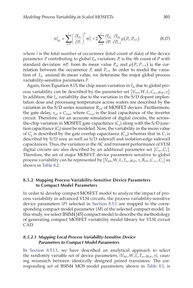
where l is the total number of occurrence (total count of data) of the device
parameter P contributing to global I ds variation; P i is the ith count of P with
standard deviation σP i from its mean value P 0 ; and ρ P P
i
i
, +
(
)
1 is the correlation between the occurrence P i and P i+1 . In order to model the variation of I ds around its mean value, we determine the major global process
variability-sensitive parameters P.
Again, from Equation 8.15, the chip mean variation in I ds due to global process variability can be described by the parameter set V W L C
th
ox
eff
0 , , , , , .
µ γ
{
}
In addition, the I ds variability due to the variation in the S/D dopant implantation dose and processing temperature across wafers are described by the
variation in the S/D series resistance R DS of MOSFET devices. Furthermore,
the gate delay, τ pd
load
C
∝
, where C load is the load capacitance of the inverter
circuit. Therefore, for an accurate simulation of digital circuits, the acrossthe-chip variation in MOSFET gate capacitance (C g ) along with the S/D junction capacitance (C J ) must be modeled. Now, the variability in the mean value
of C g is described by the gate overlap capacitance (C ov ) whereas that in C J is
described by S/D area as well as S/D sidewall and isolation-edge sidewall
capacitances. Thus, the variation in the AC and transient performance of VLSI
digital circuits are also described by an additional parameter set C C
ov
J
,
{
} .
Therefore, the set of major MOSFET device parameters sensitive to global
process variability can be represented by V W L T
R C C
th
ox
eff
D S
o v
j
0 , , , , , ,
,
,
µ γ
{
} as
shown in Table 8.2.
8.5.2 Mapping Process Variability-Sensitive Device Parameters
to Compact Model Parameters
In order to develop compact MOSFET model to analyze the impact of process variability in advanced VLSI circuits, the process variability-sensitive
device parameters { }
P selected in Section 8.5.1 are mapped to the corresponding compact model parameter { }
M of the selected compact model. In
this study, we select BSIM4 [45] compact model to describe the methodology
of generating compact MOSFET variability model library for VLSI circuit
CAD.
8.5.2.1 Mapping Local Process Variability-Sensitive Device
Parameters to Compact Model Parameters
In Section 8.5.1.1, we have described an analytical approach to select
the randomly variable set of device parameters, {
, , , , , }
V W L T
th
ox
eff
0
µ γ , causing mismatch between identically designed paired transistors. The corresponding set of BSIM4 MOS model parameters, shown in Table 8.1, is
Modeling Process Variability in Scaled MOSFETs
σ
σ
ρ
I ds
ds
i
P
ds
i
ds
i
i
l
i
l
i
i
I
P
I
P
I
P
P P
i
2
2
2
1
1
1
2
=
∂
∂
+
∂
∂
∂
∂ +
=
=
∑
∑
, + +
(
)
1
(8.17)
where l is the total number of occurrence (total count of data) of the device
parameter P contributing to global I ds variation; P i is the ith count of P with
standard deviation σP i from its mean value P 0 ; and ρ P P
i
i
, +
(
)
1 is the correlation between the occurrence P i and P i+1 . In order to model the variation of I ds around its mean value, we determine the major global process
variability-sensitive parameters P.
Again, from Equation 8.15, the chip mean variation in I ds due to global process variability can be described by the parameter set V W L C
th
ox
eff
0 , , , , , .
µ γ
{
}
In addition, the I ds variability due to the variation in the S/D dopant implantation dose and processing temperature across wafers are described by the
variation in the S/D series resistance R DS of MOSFET devices. Furthermore,
the gate delay, τ pd
load
C
∝
, where C load is the load capacitance of the inverter
circuit. Therefore, for an accurate simulation of digital circuits, the acrossthe-chip variation in MOSFET gate capacitance (C g ) along with the S/D junction capacitance (C J ) must be modeled. Now, the variability in the mean value
of C g is described by the gate overlap capacitance (C ov ) whereas that in C J is
described by S/D area as well as S/D sidewall and isolation-edge sidewall
capacitances. Thus, the variation in the AC and transient performance of VLSI
digital circuits are also described by an additional parameter set C C
ov
J
,
{
} .
Therefore, the set of major MOSFET device parameters sensitive to global
process variability can be represented by V W L T
R C C
th
ox
eff
D S
o v
j
0 , , , , , ,
,
,
µ γ
{
} as
shown in Table 8.2.
8.5.2 Mapping Process Variability-Sensitive Device Parameters
to Compact Model Parameters
In order to develop compact MOSFET model to analyze the impact of process variability in advanced VLSI circuits, the process variability-sensitive
device parameters { }
P selected in Section 8.5.1 are mapped to the corresponding compact model parameter { }
M of the selected compact model. In
this study, we select BSIM4 [45] compact model to describe the methodology
of generating compact MOSFET variability model library for VLSI circuit
CAD.
8.5.2.1 Mapping Local Process Variability-Sensitive Device
Parameters to Compact Model Parameters
In Section 8.5.1.1, we have described an analytical approach to select
the randomly variable set of device parameters, {
, , , , , }
V W L T
th
ox
eff
0
µ γ , causing mismatch between identically designed paired transistors. The corresponding set of BSIM4 MOS model parameters, shown in Table 8.1, is