

300
Compact Models for Integrated Circuit Design
location of devices [7,8]. The global variation shifts the average or mean
value of device performance. As a result, a device parameter within a chip
varies for two identically designed devices. For a large count of P from a
large number of on-chip measurement data, P converges to a Gaussian distribution with mean value P 0 and standard deviation σ = ∆P. Then the chip
mean variation in I ds due to global process variability-sensitive parameter P
is given by [9]
0
1.E+16
1.E+17
1.E+18
1.E+19
Depletion width
Channel doping concentration (cm
−3
)
10
20
30
Depth in silicon (nm)
40
X d1 @ V bs1
X d3
X d2
X d1
| V bs1 | <|V bs2 | <|V bs3 |
X d2 @ V bs2
X d3 @ V bs3
where
50
60
|
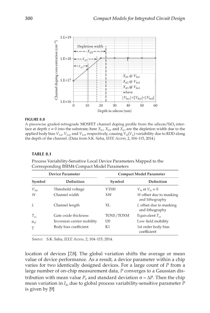
FIGURE 8.8
A piecewise graded-retrograde MOSFET channel doping profile from the silicon/SiO 2 interface at depth x = 0 into the substrate; here X d1 , X d2 , and X d3 are the depletion width due to the
applied body bias V bs1 , V bs2 , and V bs3 , respectively, causing V th (V bs ) variability due to RDD along
the depth of the channel. (Data from S.K. Saha, IEEE Access, 2, 104–115, 2014.)
TABLE 8.1
Process Variability-Sensitive Local Device Parameters Mapped to the
Corresponding BSIM4 Compact Model Parameters
Device Parameter
Compact Model Parameter
Symbol
Definition
Symbol
Definition
V th0
Threshold voltage
VTH0
V th at V bs = 0
W
Channel width
XW
W offset due to masking
and lithography
L
Channel length
XL
L offset due to masking
and lithography
T ox
Gate oxide thickness
TOXE/TOXM
Equivalent T ox
µ eff
Inversion carrier mobility
U0
Low field mobility
γ
Body bias coefficient
K1
1st order body bias
coefficient
Source: S.K. Saha, IEEE Access, 2, 104–115, 2014.
Compact Models for Integrated Circuit Design
location of devices [7,8]. The global variation shifts the average or mean
value of device performance. As a result, a device parameter within a chip
varies for two identically designed devices. For a large count of P from a
large number of on-chip measurement data, P converges to a Gaussian distribution with mean value P 0 and standard deviation σ = ∆P. Then the chip
mean variation in I ds due to global process variability-sensitive parameter P
is given by [9]
0
1.E+16
1.E+17
1.E+18
1.E+19
Depletion width
Channel doping concentration (cm
−3
)
10
20
30
Depth in silicon (nm)
40
X d1 @ V bs1
X d3
X d2
X d1
| V bs1 | <|V bs2 | <|V bs3 |
X d2 @ V bs2
X d3 @ V bs3
where
50
60
|
FIGURE 8.8
A piecewise graded-retrograde MOSFET channel doping profile from the silicon/SiO 2 interface at depth x = 0 into the substrate; here X d1 , X d2 , and X d3 are the depletion width due to the
applied body bias V bs1 , V bs2 , and V bs3 , respectively, causing V th (V bs ) variability due to RDD along
the depth of the channel. (Data from S.K. Saha, IEEE Access, 2, 104–115, 2014.)
TABLE 8.1
Process Variability-Sensitive Local Device Parameters Mapped to the
Corresponding BSIM4 Compact Model Parameters
Device Parameter
Compact Model Parameter
Symbol
Definition
Symbol
Definition
V th0
Threshold voltage
VTH0
V th at V bs = 0
W
Channel width
XW
W offset due to masking
and lithography
L
Channel length
XL
L offset due to masking
and lithography
T ox
Gate oxide thickness
TOXE/TOXM
Equivalent T ox
µ eff
Inversion carrier mobility
U0
Low field mobility
γ
Body bias coefficient
K1
1st order body bias
coefficient
Source: S.K. Saha, IEEE Access, 2, 104–115, 2014.