

299
Modeling Process Variability in Scaled MOSFETs
σ
σ
∆
∆
I ds I ds
ds
ds
i
P
i
l
ds
ds
i
ds
I
I
P
I
I
P
I
P
i
/
2
2
2
1
2
1
2
=
∂
∂
+
∂
∂
∂
∂
=
∑
i i
i
i
i
l
P P
+
+
=
(
)
∑
1
1
1
ρ ∆ ∆
,
(8.16)
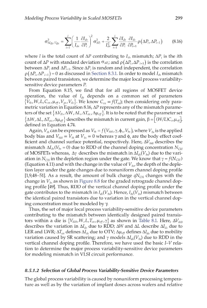
where l is the total count of ∆P contributing to I ds mismatch; ∆P i is the ith
count of ∆P with standard deviation σ ∆Pi ; and ρ ∆ ∆
P P
i
i
,
+
(
)
1 is the correlation
between ∆P i and ∆P i+1 . Since ∆P i is random and independent, the correlation
ρ ∆ ∆
P P
i
i
,
+
(
)=
1
0 as discussed in Section 8.3.1. In order to model I ds mismatch
between paired transistors, we determine the major local process variabilitysensitive device parameters P.
From Equation 8.15, we find that for all regions of MOSFET device
operation, the value of I ds depends on a common set of parameters
V W L C
V V
th
ox
eff
g s
ds
, , , , , ,
.
µ
{
} We know C ox = f(T ox ); then considering only parametric variation in Equation 8.16, ∆P represents any of the mismatch parameters of the set ∆
∆ ∆ ∆
∆
V
W L T
th
ox
eff
,
, ,
, µ
{
} . It is to be noted that the parameter set
∆ ∆ ∆
∆
W L T ox
eff
, ,
, µ
{
} describes the mismatch in current gain, β
µ
=
( / )
W L C ox eff ,
defined in Equation 4.74.
Again, V th can be expressed as V
f V
V
th
th
s
bs
= (
)
0 , , ,
γ φ
, where V bs is the applied
body bias and V th0 = V th at V bs = 0 whereas γ and f s are the body effect coefficient and channel surface potential, respectively. Here, ∆V th0 describes the
mismatch ∆I V
ds
bs
(
)
= 0 due to RDD of the channel doping concentration N CH
of MOSFETs whereas, ∆γ describes the mismatch in ∆I ds (V bs ) due to the variation in N CH in the depletion region under the gate. We know that γ = f N CH
(
)
(Equation 4.11) and with the change in the value of V bs , the depth of the depletion layer under the gate changes due to nonuniform channel doping profile
[1,9,48–51]. As a result, the amount of bulk charge qN CH changes with the
change in V bs as shown in Figure 8.8 for the graded retrograde channel doping profile [49]. Thus, RDD of the vertical channel doping profile under the
gate contributes to the mismatch in I ds (V bs ). Hence, I ds (V bs ) mismatch between
the identical paired transistors due to variation in the vertical channel doping concentration must be modeled by γ.
Thus, the set of major local process variability-sensitive device parameters
contributing to the mismatch between identically designed paired transistors within a die is V W L T
th
ox
eff
0 , , , , ,
µ γ
{
} as shown in Table 8.1. Here, ∆V th0
describes the variation in ∆I ds due to RDD; ∆W and ∆L describe ∆I ds due to
LER and LWR; ∆T ox defines ∆I ds due to OTV; ∆µ eff defines ∆I ds due to mobility
variation caused by SR scattering; and γ models ΔI ds (V bs ) due to RDD in the
vertical channel doping profile. Therefore, we have used the basic I–V relation to determine the major process variability-sensitive device parameters
for modeling mismatch in VLSI circuit performance.
8.5.1.2 Selection of Global Process Variability-Sensitive Device Parameters
The global process variability is caused by nonuniform processing temperature as well as by the variation of implant doses across wafers and relative
Modeling Process Variability in Scaled MOSFETs
σ
σ
∆
∆
I ds I ds
ds
ds
i
P
i
l
ds
ds
i
ds
I
I
P
I
I
P
I
P
i
/
2
2
2
1
2
1
2
=
∂
∂
+
∂
∂
∂
∂
=
∑
i i
i
i
i
l
P P
+
+
=
(
)
∑
1
1
1
ρ ∆ ∆
,
(8.16)
where l is the total count of ∆P contributing to I ds mismatch; ∆P i is the ith
count of ∆P with standard deviation σ ∆Pi ; and ρ ∆ ∆
P P
i
i
,
+
(
)
1 is the correlation
between ∆P i and ∆P i+1 . Since ∆P i is random and independent, the correlation
ρ ∆ ∆
P P
i
i
,
+
(
)=
1
0 as discussed in Section 8.3.1. In order to model I ds mismatch
between paired transistors, we determine the major local process variabilitysensitive device parameters P.
From Equation 8.15, we find that for all regions of MOSFET device
operation, the value of I ds depends on a common set of parameters
V W L C
V V
th
ox
eff
g s
ds
, , , , , ,
.
µ
{
} We know C ox = f(T ox ); then considering only parametric variation in Equation 8.16, ∆P represents any of the mismatch parameters of the set ∆
∆ ∆ ∆
∆
V
W L T
th
ox
eff
,
, ,
, µ
{
} . It is to be noted that the parameter set
∆ ∆ ∆
∆
W L T ox
eff
, ,
, µ
{
} describes the mismatch in current gain, β
µ
=
( / )
W L C ox eff ,
defined in Equation 4.74.
Again, V th can be expressed as V
f V
V
th
th
s
bs
= (
)
0 , , ,
γ φ
, where V bs is the applied
body bias and V th0 = V th at V bs = 0 whereas γ and f s are the body effect coefficient and channel surface potential, respectively. Here, ∆V th0 describes the
mismatch ∆I V
ds
bs
(
)
= 0 due to RDD of the channel doping concentration N CH
of MOSFETs whereas, ∆γ describes the mismatch in ∆I ds (V bs ) due to the variation in N CH in the depletion region under the gate. We know that γ = f N CH
(
)
(Equation 4.11) and with the change in the value of V bs , the depth of the depletion layer under the gate changes due to nonuniform channel doping profile
[1,9,48–51]. As a result, the amount of bulk charge qN CH changes with the
change in V bs as shown in Figure 8.8 for the graded retrograde channel doping profile [49]. Thus, RDD of the vertical channel doping profile under the
gate contributes to the mismatch in I ds (V bs ). Hence, I ds (V bs ) mismatch between
the identical paired transistors due to variation in the vertical channel doping concentration must be modeled by γ.
Thus, the set of major local process variability-sensitive device parameters
contributing to the mismatch between identically designed paired transistors within a die is V W L T
th
ox
eff
0 , , , , ,
µ γ
{
} as shown in Table 8.1. Here, ∆V th0
describes the variation in ∆I ds due to RDD; ∆W and ∆L describe ∆I ds due to
LER and LWR; ∆T ox defines ∆I ds due to OTV; ∆µ eff defines ∆I ds due to mobility
variation caused by SR scattering; and γ models ΔI ds (V bs ) due to RDD in the
vertical channel doping profile. Therefore, we have used the basic I–V relation to determine the major process variability-sensitive device parameters
for modeling mismatch in VLSI circuit performance.
8.5.1.2 Selection of Global Process Variability-Sensitive Device Parameters
The global process variability is caused by nonuniform processing temperature as well as by the variation of implant doses across wafers and relative