

298
Compact Models for Integrated Circuit Design
mapping process-sensitive device parameters to corresponding compact
model parameters, determination of variances for mismatch modeling and
global variability modeling, and finally, building compact variability model.
The modeling methodology outlined in Figure 8.7 is described in the following section.
8.5.1 Determination of Process Variability-Sensitive
MOSFET Device Parameters
It is clear from our discussions in Section 8.2 that process variability causes
variability in MOSFET device performance, which in turn causes variability in VLSI circuit performance. Since, the MOSFET device performance is
determined by I ds , in order to determine the impact of process variability on
circuit performance, we determine the process variability-sensitive device
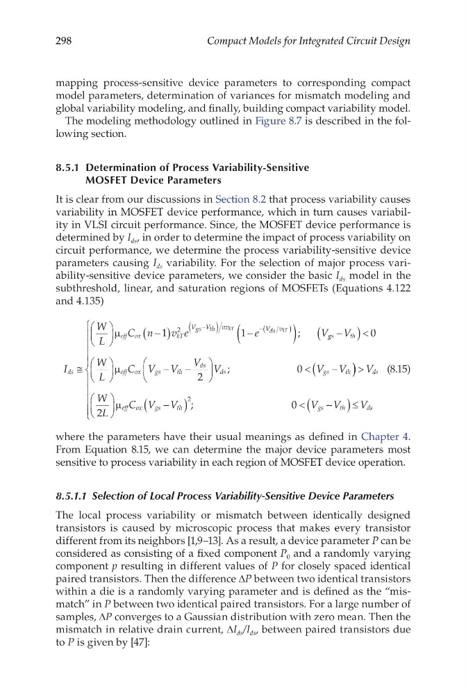
parameters causing I ds variability. For the selection of major process variability-sensitive device parameters, we consider the basic I ds model in the
subthreshold, linear, and saturation regions of MOSFETs (Equations 4.122
and 4.135)
I
W
L
C n
v e
e
V
ds
eff ox
k T
V gs V th nv
V ds v
kT
kT
≅
−
( )
−
(
)
−
(
)
−(
)
µ
1
1
2
;
g gs
th
eff ox
g s
t h
ds
ds
gs
th
V
W
L
C V V
V V
V V
−
(
) <
−
−
<
−
(
0
2
µ
;
0
) ) >
−
(
)
<
−
(
) ≤
V
W
L
C V V
V V
V
ds
eff ox
g s
t h
g s
t h
d s
2
2
µ
;
0
(8.15)
where the parameters have their usual meanings as defined in Chapter 4.
From Equation 8.15, we can determine the major device parameters most
sensitive to process variability in each region of MOSFET device operation.
8.5.1.1 Selection of Local Process Variability-Sensitive Device Parameters
The local process variability or mismatch between identically designed
transistors is caused by microscopic process that makes every transistor
different from its neighbors [1,9–13]. As a result, a device parameter P can be
considered as consisting of a fixed component P 0 and a randomly varying
component p resulting in different values of P for closely spaced identical
paired transistors. Then the difference ∆P between two identical transistors
within a die is a randomly varying parameter and is defined as the “mismatch” in P between two identical paired transistors. For a large number of
samples, ∆P converges to a Gaussian distribution with zero mean. Then the
mismatch in relative drain current, ∆I ds /I ds , between paired transistors due
to P is given by [47]:
Compact Models for Integrated Circuit Design
mapping process-sensitive device parameters to corresponding compact
model parameters, determination of variances for mismatch modeling and
global variability modeling, and finally, building compact variability model.
The modeling methodology outlined in Figure 8.7 is described in the following section.
8.5.1 Determination of Process Variability-Sensitive
MOSFET Device Parameters
It is clear from our discussions in Section 8.2 that process variability causes
variability in MOSFET device performance, which in turn causes variability in VLSI circuit performance. Since, the MOSFET device performance is
determined by I ds , in order to determine the impact of process variability on
circuit performance, we determine the process variability-sensitive device
parameters causing I ds variability. For the selection of major process variability-sensitive device parameters, we consider the basic I ds model in the
subthreshold, linear, and saturation regions of MOSFETs (Equations 4.122
and 4.135)
I
W
L
C n
v e
e
V
ds
eff ox
k T
V gs V th nv
V ds v
kT
kT
≅
−
( )
−
(
)
−
(
)
−(
)
µ
1
1
2
;
g gs
th
eff ox
g s
t h
ds
ds
gs
th
V
W
L
C V V
V V
V V
−
(
) <
−
−
<
−
(
0
2
µ
;
0
) ) >
−
(
)
<
−
(
) ≤
V
W
L
C V V
V V
V
ds
eff ox
g s
t h
g s
t h
d s
2
2
µ
;
0
(8.15)
where the parameters have their usual meanings as defined in Chapter 4.
From Equation 8.15, we can determine the major device parameters most
sensitive to process variability in each region of MOSFET device operation.
8.5.1.1 Selection of Local Process Variability-Sensitive Device Parameters
The local process variability or mismatch between identically designed
transistors is caused by microscopic process that makes every transistor
different from its neighbors [1,9–13]. As a result, a device parameter P can be
considered as consisting of a fixed component P 0 and a randomly varying
component p resulting in different values of P for closely spaced identical
paired transistors. Then the difference ∆P between two identical transistors
within a die is a randomly varying parameter and is defined as the “mismatch” in P between two identical paired transistors. For a large number of
samples, ∆P converges to a Gaussian distribution with zero mean. Then the
mismatch in relative drain current, ∆I ds /I ds , between paired transistors due
to P is given by [47]: