

289
Modeling Process Variability in Scaled MOSFETs
σ
εφ ε
V
C
q
T
N
W L
th RDD
s i B
ox
ox
CH
eff eff
,
≅ ⋅ (
)
3
4
4
(8.2)
where:
C is a number and is given by 0.8165 [23] or 0.7071 [24] with or without the
dopant variation along the depth of the channel region, respectively
q is the electronic charge
ε si and ε ox are the permittivity of silicon and silicon-dioxide (SiO 2 ),
respectively
φ B
k T
C H
i
v
N n
=
(
)
ln
/ is the bulk potential of the channel region of MOSFETs
and v kT and n i are the thermal voltage and intrinsic carrier concentration, respectively
W eff and L eff represent the effective dimension of W and L, respectively
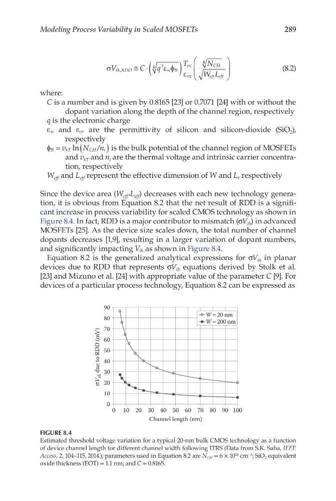
Since the device area (W eff* L eff ) decreases with each new technology generation, it is obvious from Equation 8.2 that the net result of RDD is a significant increase in process variability for scaled CMOS technology as shown in
Figure 8.4. In fact, RDD is a major contributor to mismatch (σV th ) in advanced
MOSFETs [25]. As the device size scales down, the total number of channel
dopants decreases [1,9], resulting in a larger variation of dopant numbers,
and significantly impacting V th as shown in Figure 8.4.
Equation 8.2 is the generalized analytical expressions for σV th in planar
devices due to RDD that represents σV th equations derived by Stolk et al.
[23] and Mizuno et al. [24] with appropriate value of the parameter C [9]. For
devices of a particular process technology, Equation 8.2 can be expressed as
0
0
10
20
30
40
50
60
70
σV
th due to RDD (mV)
80
90
W = 20 nm
W = 200 nm
10 20 30 40
Channel length (nm)
50 60 70 80 90 100
FIGURE 8.4
Estimated threshold voltage variation for a typical 20-nm bulk CMOS technology as a function
of device channel length for different channel width following ITRS (Data from S.K. Saha, IEEE
Access, 2, 104–115, 2014.); parameters used in Equation 8.2 are N CH = 6 × 10 18 cm −3 ; SiO 2 equivalent
oxide thickness (EOT) = 1.1 nm; and C = 0.8165.
Modeling Process Variability in Scaled MOSFETs
σ
εφ ε
V
C
q
T
N
W L
th RDD
s i B
ox
ox
CH
eff eff
,
≅ ⋅ (
)
3
4
4
(8.2)
where:
C is a number and is given by 0.8165 [23] or 0.7071 [24] with or without the
dopant variation along the depth of the channel region, respectively
q is the electronic charge
ε si and ε ox are the permittivity of silicon and silicon-dioxide (SiO 2 ),
respectively
φ B
k T
C H
i
v
N n
=
(
)
ln
/ is the bulk potential of the channel region of MOSFETs
and v kT and n i are the thermal voltage and intrinsic carrier concentration, respectively
W eff and L eff represent the effective dimension of W and L, respectively
Since the device area (W eff* L eff ) decreases with each new technology generation, it is obvious from Equation 8.2 that the net result of RDD is a significant increase in process variability for scaled CMOS technology as shown in
Figure 8.4. In fact, RDD is a major contributor to mismatch (σV th ) in advanced
MOSFETs [25]. As the device size scales down, the total number of channel
dopants decreases [1,9], resulting in a larger variation of dopant numbers,
and significantly impacting V th as shown in Figure 8.4.
Equation 8.2 is the generalized analytical expressions for σV th in planar
devices due to RDD that represents σV th equations derived by Stolk et al.
[23] and Mizuno et al. [24] with appropriate value of the parameter C [9]. For
devices of a particular process technology, Equation 8.2 can be expressed as
0
0
10
20
30
40
50
60
70
σV
th due to RDD (mV)
80
90
W = 20 nm
W = 200 nm
10 20 30 40
Channel length (nm)
50 60 70 80 90 100
FIGURE 8.4
Estimated threshold voltage variation for a typical 20-nm bulk CMOS technology as a function
of device channel length for different channel width following ITRS (Data from S.K. Saha, IEEE
Access, 2, 104–115, 2014.); parameters used in Equation 8.2 are N CH = 6 × 10 18 cm −3 ; SiO 2 equivalent
oxide thickness (EOT) = 1.1 nm; and C = 0.8165.