

288
Compact Models for Integrated Circuit Design
region is doped with dopant atoms to control its threshold voltage (V th ) [5–8].
For a device with channel doping concentration N CH and source/drain (S/D)
junction depth X j , the total number of dopant atoms in the channel region is
given by [1,9]:
N
N W L X
CHtotal
C H
j
≅
⋅ ⋅
⋅
(8.1)
Equation 8.1 shows that the continuous scaling down of L, W, and X j causes
the total number of dopants in the channel to decrease, despite the corresponding increase in the channel-doping concentration according to the
CMOS scaling rule [2,3]. Using Equation 8.1 and the target specifications for
advanced CMOS technology scaling by International Technology Roadmap for
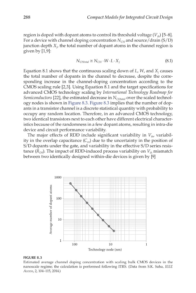
Semiconductors [22], the estimated decrease in N CHtotal over the scaled technology nodes is shown in Figure 8.3. Figure 8.3 implies that the number of dopants in a transistor channel is a discrete statistical quantity with probability to
occupy any random location. Therefore, in an advanced CMOS technology,
two identical transistors next to each other have different electrical characteristics because of the randomness in a few dopant atoms, resulting in intra-die
device and circuit performance variability.
The major effects of RDD include significant variability in V th , variability in the overlap capacitance (C ov ) due to the uncertainty in the position of
S/D dopants under the gate, and variability in the effective S/D series resistance (R DS ). The impact of RDD-induced process variability on V th mismatch
between two identically designed within-die devices is given by [9]
100
1
10
100
Average number of dopant atoms
1000
10
Technology node (nm)
1
FIGURE 8.3
Estimated average channel doping concentration with scaling bulk CMOS devices in the
nanoscale regime; the calculation is performed following ITRS. (Data from S.K. Saha, IEEE
Access, 2, 104–115, 2014.)
Compact Models for Integrated Circuit Design
region is doped with dopant atoms to control its threshold voltage (V th ) [5–8].
For a device with channel doping concentration N CH and source/drain (S/D)
junction depth X j , the total number of dopant atoms in the channel region is
given by [1,9]:
N
N W L X
CHtotal
C H
j
≅
⋅ ⋅
⋅
(8.1)
Equation 8.1 shows that the continuous scaling down of L, W, and X j causes
the total number of dopants in the channel to decrease, despite the corresponding increase in the channel-doping concentration according to the
CMOS scaling rule [2,3]. Using Equation 8.1 and the target specifications for
advanced CMOS technology scaling by International Technology Roadmap for
Semiconductors [22], the estimated decrease in N CHtotal over the scaled technology nodes is shown in Figure 8.3. Figure 8.3 implies that the number of dopants in a transistor channel is a discrete statistical quantity with probability to
occupy any random location. Therefore, in an advanced CMOS technology,
two identical transistors next to each other have different electrical characteristics because of the randomness in a few dopant atoms, resulting in intra-die
device and circuit performance variability.
The major effects of RDD include significant variability in V th , variability in the overlap capacitance (C ov ) due to the uncertainty in the position of
S/D dopants under the gate, and variability in the effective S/D series resistance (R DS ). The impact of RDD-induced process variability on V th mismatch
between two identically designed within-die devices is given by [9]
100
1
10
100
Average number of dopant atoms
1000
10
Technology node (nm)
1
FIGURE 8.3
Estimated average channel doping concentration with scaling bulk CMOS devices in the
nanoscale regime; the calculation is performed following ITRS. (Data from S.K. Saha, IEEE
Access, 2, 104–115, 2014.)