

283
Compact MOSFET Models for RF Applications
7.4.3 MOSFET RF Model for GHz Applications
Using the lumped gate resistance and the substrate resistance network
models described earlier, a unified compact device model can be realized
for simulations of both RF and baseband analog circuits. The equivalent
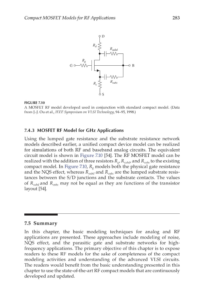
circuit model is shown in Figure 7.10 [54]. The RF MOSFET model can be
realized with the addition of three resistors R g , R subd , and R subs to the existing
compact model. In Figure 7.10, R g models both the physical gate resistance
and the NQS effect, whereas R subd and R subs are the lumped substrate resistances between the S/D junctions and the substrate contacts. The values
of R subd and R subs may not be equal as they are functions of the transistor
layout [54].
7.5 Summary
In this chapter, the basic modeling techniques for analog and RF
applications are presented. These approaches include modeling of noise,
NQS effect, and the parasitic gate and substrate networks for highfrequency applications. The primary objective of this chapter is to expose
readers to these RF models for the sake of completeness of the compact
modeling activities and understanding of the advanced VLSI circuits.
The readers would benefit from the basic understanding presented in this
chapter to use the state-of-the-art RF compact models that are continuously
developed and updated.
D
R d
R g
G
B
S
R subd
R subs
R s
FIGURE 7.10
A MOSFET RF model developed used in conjunction with standard compact model. (Data
from J.-J. Ou et al., IEEE Symposium on VLSI Technology, 94–95, 1998.)
Compact MOSFET Models for RF Applications
7.4.3 MOSFET RF Model for GHz Applications
Using the lumped gate resistance and the substrate resistance network
models described earlier, a unified compact device model can be realized
for simulations of both RF and baseband analog circuits. The equivalent
circuit model is shown in Figure 7.10 [54]. The RF MOSFET model can be
realized with the addition of three resistors R g , R subd , and R subs to the existing
compact model. In Figure 7.10, R g models both the physical gate resistance
and the NQS effect, whereas R subd and R subs are the lumped substrate resistances between the S/D junctions and the substrate contacts. The values
of R subd and R subs may not be equal as they are functions of the transistor
layout [54].
7.5 Summary
In this chapter, the basic modeling techniques for analog and RF
applications are presented. These approaches include modeling of noise,
NQS effect, and the parasitic gate and substrate networks for highfrequency applications. The primary objective of this chapter is to expose
readers to these RF models for the sake of completeness of the compact
modeling activities and understanding of the advanced VLSI circuits.
The readers would benefit from the basic understanding presented in this
chapter to use the state-of-the-art RF compact models that are continuously
developed and updated.
D
R d
R g
G
B
S
R subd
R subs
R s
FIGURE 7.10
A MOSFET RF model developed used in conjunction with standard compact model. (Data
from J.-J. Ou et al., IEEE Symposium on VLSI Technology, 94–95, 1998.)