

282
Compact Models for Integrated Circuit Design
Thus, the overall channel resistance seen from the gate is
1
1
1
R
R
R
gch
s t
e d
=
+
γ
(7.56)
where:
γ is a parameter accounting for the distributed nature of the channel
resistance
It is shown that if the resistance is uniformly distributed along the channel, the value of γ is 12 [58]. However, this assumption is true only in the
saturation region; therefore, γ is used as a fitting parameter. Thus, from
Equations 7.53 and 7.56 (along with Equation 7.52), we can model the effective gate resistance network for RF application. The reported simulation
results using the above-described model show very good agreement with
the data obtained by numerical device simulation.
7.4.2 Modeling Substrate Network
Modeling of the substrate parasitic elements and substrate network is very
important for RF applications of MOSFET devices [40,59]. In order to obtain
the desired scalable RF model, it is critical to develop scalable model for each
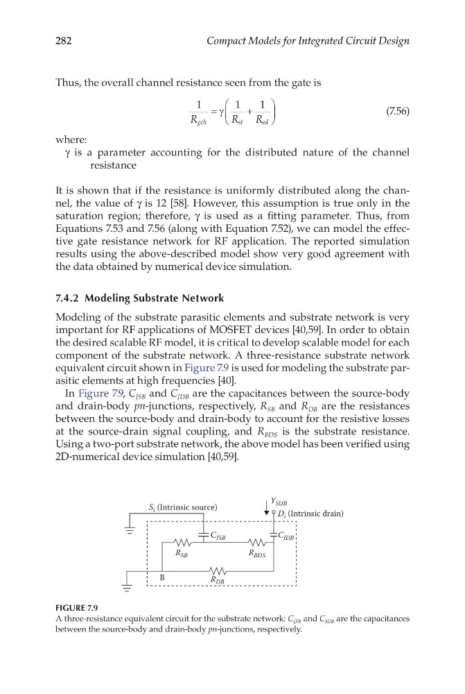
component of the substrate network. A three-resistance substrate network
equivalent circuit shown in Figure 7.9 is used for modeling the substrate parasitic elements at high frequencies [40].
In Figure 7.9, C JSB and C JDB are the capacitances between the source-body
and drain-body pn-junctions, respectively, R SB and R DB are the resistances
between the source-body and drain-body to account for the resistive losses
at the source-drain signal coupling, and R BDS is the substrate resistance.
Using a two-port substrate network, the above model has been verified using
2D-numerical device simulation [40,59].
S i (Intrinsic source)
D i (Intrinsic drain)
Y SUB
C JSB
C JDB
R BDS
R SB
R DB
B
FIGURE 7.9
A three-resistance equivalent circuit for the substrate network: C JSB and C JDB are the capacitances
between the source-body and drain-body pn-junctions, respectively.
Compact Models for Integrated Circuit Design
Thus, the overall channel resistance seen from the gate is
1
1
1
R
R
R
gch
s t
e d
=
+
γ
(7.56)
where:
γ is a parameter accounting for the distributed nature of the channel
resistance
It is shown that if the resistance is uniformly distributed along the channel, the value of γ is 12 [58]. However, this assumption is true only in the
saturation region; therefore, γ is used as a fitting parameter. Thus, from
Equations 7.53 and 7.56 (along with Equation 7.52), we can model the effective gate resistance network for RF application. The reported simulation
results using the above-described model show very good agreement with
the data obtained by numerical device simulation.
7.4.2 Modeling Substrate Network
Modeling of the substrate parasitic elements and substrate network is very
important for RF applications of MOSFET devices [40,59]. In order to obtain
the desired scalable RF model, it is critical to develop scalable model for each
component of the substrate network. A three-resistance substrate network
equivalent circuit shown in Figure 7.9 is used for modeling the substrate parasitic elements at high frequencies [40].
In Figure 7.9, C JSB and C JDB are the capacitances between the source-body
and drain-body pn-junctions, respectively, R SB and R DB are the resistances
between the source-body and drain-body to account for the resistive losses
at the source-drain signal coupling, and R BDS is the substrate resistance.
Using a two-port substrate network, the above model has been verified using
2D-numerical device simulation [40,59].
S i (Intrinsic source)
D i (Intrinsic drain)
Y SUB
C JSB
C JDB
R BDS
R SB
R DB
B
FIGURE 7.9
A three-resistance equivalent circuit for the substrate network: C JSB and C JDB are the capacitances
between the source-body and drain-body pn-junctions, respectively.