

270
Compact Models for Integrated Circuit Design
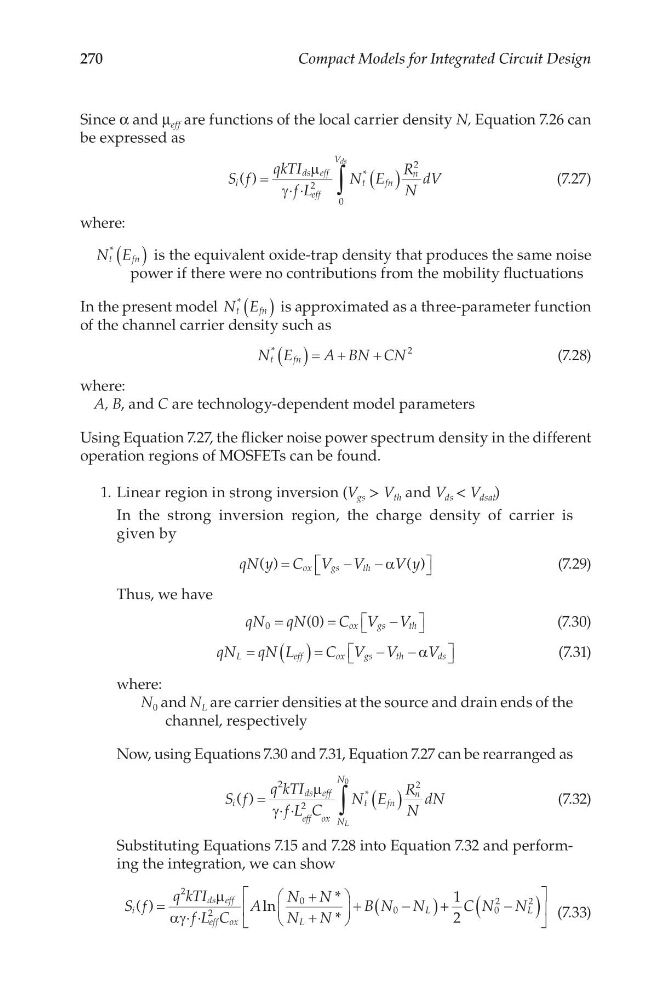
Since α and μ eff are functions of the local carrier density N, Equation 7.26 can
be expressed as
S f
qkTI
f L
N E
R
N
dV
i
ds eff
eff
t
V
fn
n
ds
( )
*
= ⋅ ⋅
( )
∫
µ
γ
2
0
2
(7.27)
where:
N E
t
f n
*
( ) is the equivalent oxide-trap density that produces the same noise
power if there were no contributions from the mobility fluctuations
In the present model N E
t
f n
*
( ) is approximated as a three-parameter function
of the channel carrier density such as
N E
A BN CN
t
f n
*
( ) = + +
2
(7.28)
where:
A, B, and C are technology-dependent model parameters
Using Equation 7.27, the flicker noise power spectrum density in the different
operation regions of MOSFETs can be found.
1. Linear region in strong inversion (V gs > V th and V ds < V dsat )
In the strong inversion region, the charge density of carrier is
given by
qN y C V V
V y
ox
gs
th
( )
( )
=
−
−
α
(7.29)
Thus, we have
qN qN
C V V
ox
gs
th
0
0
=
=
−
( )
(7.30)
qN qN L
C V V
V
L
e ff
ox
gs
th
ds
=
( ) =
−
−
α
(7.31)
where:
N 0 and N L are carrier densities at the source and drain ends of the
channel, respectively
Now, using Equations 7.30 and 7.31, Equation 7.27 can be rearranged as
S f
q kTI
f L C
N E
R
N
dN
i
ds eff
eff ox
t
N
N
fn
n
L
( )
*
= ⋅ ⋅
( )
∫
2
2
2
0
µ
γ
(7.32)
Substituting Equations 7.15 and 7.28 into Equation 7.32 and performing the integration, we can show
S f
q kTI
f L C
A
N N
N N
B N N
i
ds eff
eff ox
L
L
( )
ln
*
*
= ⋅ ⋅
+
+
+
−
(
)
2
2
0
0
µ
αγ
+ +
−
(
)
1
2
0
2
2
C N N L
(7.33)
Compact Models for Integrated Circuit Design
Since α and μ eff are functions of the local carrier density N, Equation 7.26 can
be expressed as
S f
qkTI
f L
N E
R
N
dV
i
ds eff
eff
t
V
fn
n
ds
( )
*
= ⋅ ⋅
( )
∫
µ
γ
2
0
2
(7.27)
where:
N E
t
f n
*
( ) is the equivalent oxide-trap density that produces the same noise
power if there were no contributions from the mobility fluctuations
In the present model N E
t
f n
*
( ) is approximated as a three-parameter function
of the channel carrier density such as
N E
A BN CN
t
f n
*
( ) = + +
2
(7.28)
where:
A, B, and C are technology-dependent model parameters
Using Equation 7.27, the flicker noise power spectrum density in the different
operation regions of MOSFETs can be found.
1. Linear region in strong inversion (V gs > V th and V ds < V dsat )
In the strong inversion region, the charge density of carrier is
given by
qN y C V V
V y
ox
gs
th
( )
( )
=
−
−
α
(7.29)
Thus, we have
qN qN
C V V
ox
gs
th
0
0
=
=
−
( )
(7.30)
qN qN L
C V V
V
L
e ff
ox
gs
th
ds
=
( ) =
−
−
α
(7.31)
where:
N 0 and N L are carrier densities at the source and drain ends of the
channel, respectively
Now, using Equations 7.30 and 7.31, Equation 7.27 can be rearranged as
S f
q kTI
f L C
N E
R
N
dN
i
ds eff
eff ox
t
N
N
fn
n
L
( )
*
= ⋅ ⋅
( )
∫
2
2
2
0
µ
γ
(7.32)
Substituting Equations 7.15 and 7.28 into Equation 7.32 and performing the integration, we can show
S f
q kTI
f L C
A
N N
N N
B N N
i
ds eff
eff ox
L
L
( )
ln
*
*
= ⋅ ⋅
+
+
+
−
(
)
2
2
0
0
µ
αγ
+ +
−
(
)
1
2
0
2
2
C N N L
(7.33)