

255
MOSFET Capacitance Models
τ
τ
r
q s t
N
>
(6.100)
where:
N qs is a factor with a value between 15 and 25, depending on the application
τ t is defined as the average time taken by an inversion carrier to travel the
length of the channel
that is,
τ t
I
ds
Q
I
=
(6.101)
Now using Q I from Equation 6.61 and saturation region I ds from Equation 4.100,
we get
τ
α µ
α µ
t
s
g s
t h
sdsat
L
V V
L
V
=
−
(
)
=
4
3
4
3
2
2
(6.102)
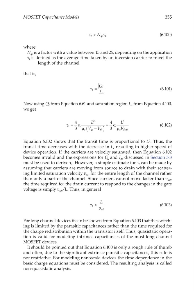
Equation 6.102 shows that the transit time is proportional to L 2 . Thus, the
transit time decreases with the decrease in L, resulting in higher speed of
device operation. If the carriers are velocity saturated, then Equation 6.102
becomes invalid and the expressions for Q I and I ds discussed in Section 5.3
must be used to derive τ t . However, a simple estimate for τ t can be made by
assuming that carriers are moving from source to drain with their scattering limited saturation velocity v sat for the entire length of the channel rather
than only a part of the channel. Since carriers cannot move faster than v sat ,
the time required for the drain current to respond to the changes in the gate
voltage is simply v sat /L. Thus, in general
τ t
L
v
>
sat
(6.103)
For long channel devices it can be shown from Equation 6.103 that the switching is limited by the parasitic capacitances rather than the time required for
the charge redistribution within the transistor itself. Thus, quasistatic operation is valid for modeling intrinsic capacitances of the most long channel
MOSFET devices.
It should be pointed out that Equation 6.100 is only a rough rule of thumb
and often, due to the significant extrinsic parasitic capacitances, this rule is
not restrictive. For modeling nanoscale devices the time dependence in the
basic charge equations must be considered. The resulting analysis is called
non-quasistatic analysis.
MOSFET Capacitance Models
τ
τ
r
q s t
N
>
(6.100)
where:
N qs is a factor with a value between 15 and 25, depending on the application
τ t is defined as the average time taken by an inversion carrier to travel the
length of the channel
that is,
τ t
I
ds
Q
I
=
(6.101)
Now using Q I from Equation 6.61 and saturation region I ds from Equation 4.100,
we get
τ
α µ
α µ
t
s
g s
t h
sdsat
L
V V
L
V
=
−
(
)
=
4
3
4
3
2
2
(6.102)
Equation 6.102 shows that the transit time is proportional to L 2 . Thus, the
transit time decreases with the decrease in L, resulting in higher speed of
device operation. If the carriers are velocity saturated, then Equation 6.102
becomes invalid and the expressions for Q I and I ds discussed in Section 5.3
must be used to derive τ t . However, a simple estimate for τ t can be made by
assuming that carriers are moving from source to drain with their scattering limited saturation velocity v sat for the entire length of the channel rather
than only a part of the channel. Since carriers cannot move faster than v sat ,
the time required for the drain current to respond to the changes in the gate
voltage is simply v sat /L. Thus, in general
τ t
L
v
>
sat
(6.103)
For long channel devices it can be shown from Equation 6.103 that the switching is limited by the parasitic capacitances rather than the time required for
the charge redistribution within the transistor itself. Thus, quasistatic operation is valid for modeling intrinsic capacitances of the most long channel
MOSFET devices.
It should be pointed out that Equation 6.100 is only a rough rule of thumb
and often, due to the significant extrinsic parasitic capacitances, this rule is
not restrictive. For modeling nanoscale devices the time dependence in the
basic charge equations must be considered. The resulting analysis is called
non-quasistatic analysis.