

254
Compact Models for Integrated Circuit Design
V
V
V
V
V
gs,overlap
gs
gs
gd,overlap
gd
=
+
(
) −
+
(
) +
=
1
2
4
1
2
1
1
1
δ
δ
δ
+ +
(
) −
+
(
) +
δ
δ
δ
2
2
2
4
V gd
(6.96)
where:
δ 1 = δ 2 = 0.02 V
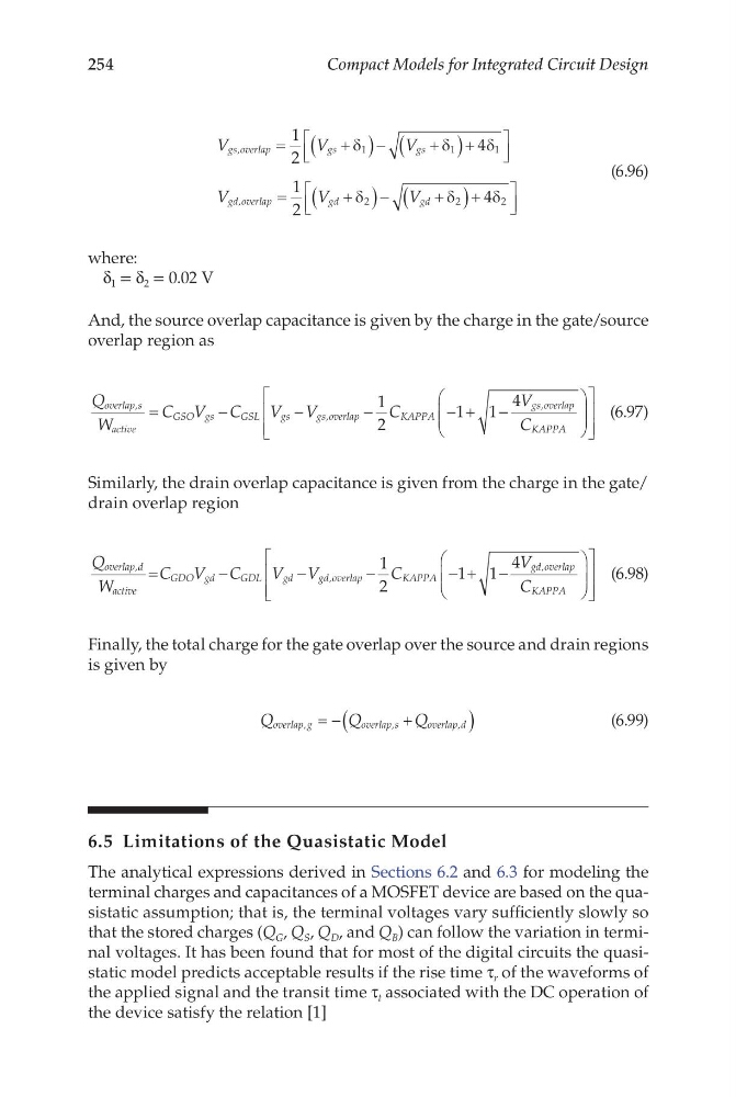
And, the source overlap capacitance is given by the charge in the gate/source
overlap region as
Q
W
C V C
V V
C
overlap,s
active
GSO gs
G SL
gs
gs,overlap
KAPPA
=
−
−
−
− +
1
2
1 1− −
4V
C
gs,overlap
KAPPA
(6.97)
Similarly, the drain overlap capacitance is given from the charge in the gate/
drain overlap region
Q
W
C V C
V V
C
overlap,d
active
GDO gd
G DL
gd
gd,overlap
KAPPA
=
−
−
−
− +
1
2
1 1− −
4V
C
gd,overlap
KAPPA
(6.98)
Finally, the total charge for the gate overlap over the source and drain regions
is given by
Q
Q
Q
overlap,g
overlap,s
overlap,d
= −
+
(
)
(6.99)
6.5 Limitations of the Quasistatic Model
The analytical expressions derived in Sections 6.2 and 6.3 for modeling the
terminal charges and capacitances of a MOSFET device are based on the quasistatic assumption; that is, the terminal voltages vary sufficiently slowly so
that the stored charges (Q G , Q S , Q D , and Q B ) can follow the variation in terminal voltages. It has been found that for most of the digital circuits the quasistatic model predicts acceptable results if the rise time τ r of the waveforms of
the applied signal and the transit time τ t associated with the DC operation of
the device satisfy the relation [1]
Compact Models for Integrated Circuit Design
V
V
V
V
V
gs,overlap
gs
gs
gd,overlap
gd
=
+
(
) −
+
(
) +
=
1
2
4
1
2
1
1
1
δ
δ
δ
+ +
(
) −
+
(
) +
δ
δ
δ
2
2
2
4
V gd
(6.96)
where:
δ 1 = δ 2 = 0.02 V
And, the source overlap capacitance is given by the charge in the gate/source
overlap region as
Q
W
C V C
V V
C
overlap,s
active
GSO gs
G SL
gs
gs,overlap
KAPPA
=
−
−
−
− +
1
2
1 1− −
4V
C
gs,overlap
KAPPA
(6.97)
Similarly, the drain overlap capacitance is given from the charge in the gate/
drain overlap region
Q
W
C V C
V V
C
overlap,d
active
GDO gd
G DL
gd
gd,overlap
KAPPA
=
−
−
−
− +
1
2
1 1− −
4V
C
gd,overlap
KAPPA
(6.98)
Finally, the total charge for the gate overlap over the source and drain regions
is given by
Q
Q
Q
overlap,g
overlap,s
overlap,d
= −
+
(
)
(6.99)
6.5 Limitations of the Quasistatic Model
The analytical expressions derived in Sections 6.2 and 6.3 for modeling the
terminal charges and capacitances of a MOSFET device are based on the quasistatic assumption; that is, the terminal voltages vary sufficiently slowly so
that the stored charges (Q G , Q S , Q D , and Q B ) can follow the variation in terminal voltages. It has been found that for most of the digital circuits the quasistatic model predicts acceptable results if the rise time τ r of the waveforms of
the applied signal and the transit time τ t associated with the DC operation of
the device satisfy the relation [1]