

253
MOSFET Capacitance Models
that if the overlap distance l ov approaches zero, there will be an overlap
capacitance present in MOSFET devices due to the fringing components
C fo and C fi .
Although, the inner fringing capacitance C fi is found to be gate and drain
bias dependent, C fi calculated from Equation 6.90 is its maximum value. The
value of C fi decreases with the increase in the gate voltage from the subthreshold to strong inversion and approaches to zero in strong saturation.
The overlap capacitance is bias dependent, particularly for advance CMOS
(complementary metal-oxide-semiconductor) technology and thin gate oxide
devices.
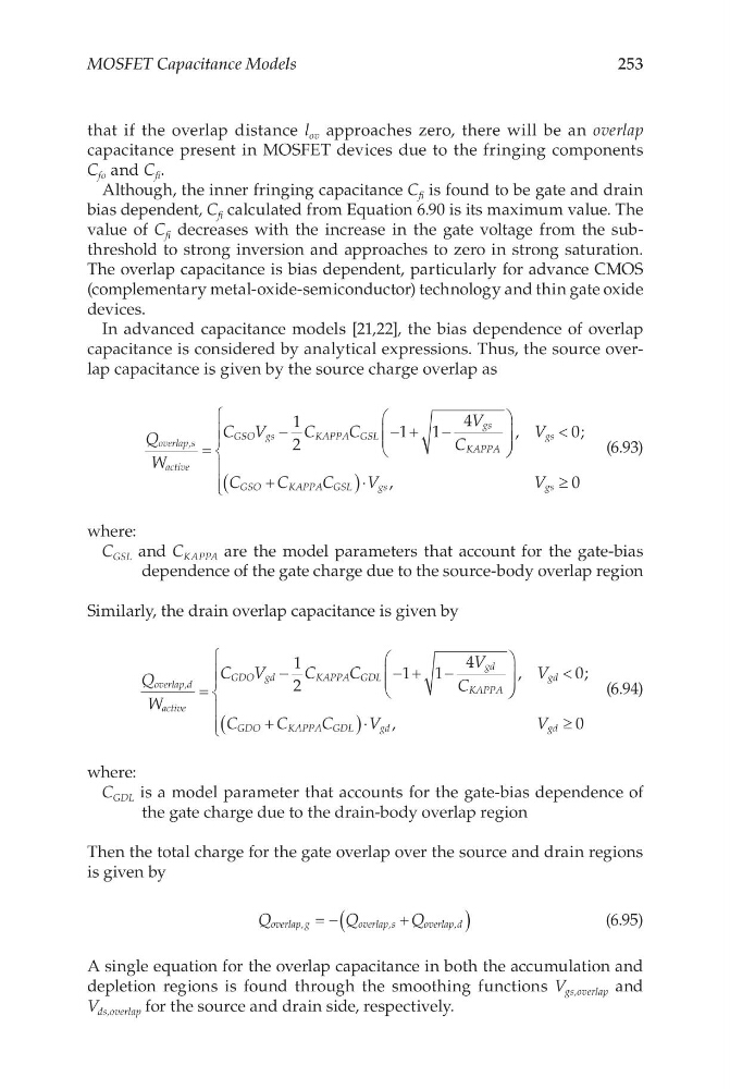
In advanced capacitance models [21,22], the bias dependence of overlap
capacitance is considered by analytical expressions. Thus, the source overlap capacitance is given by the source charge overlap as
Q
W
C V
C
C
V
C
GSO gs
K APPA GSL
gs
KAPPA
overlap,s
active
=
−
−+ −
1
2
1 1
4
<
+
(
) ⋅
≥
,
,
V
C
C
C
V
V
gs
GSO
K APPA GSL
g s
g s
0
0
;
(6.93)
where:
C GSL and C KAPPA are the model parameters that account for the gate-bias
dependence of the gate charge due to the source-body overlap region
Similarly, the drain overlap capacitance is given by
Q
W
C V
C
C
V
C
GDO gd
K APPA GDL
gd
KAPPA
overlap,d
active
=
−
−+ −
1
2
1 1
4
<
+
(
) ⋅
≥
,
,
V
C
C
C
V
V
gd
GDO
K APPA GDL
g d
g d
0
0
;
(6.94)
where:
C GDL is a model parameter that accounts for the gate-bias dependence of
the gate charge due to the drain-body overlap region
Then the total charge for the gate overlap over the source and drain regions
is given by
Q
Q
Q
overlap,g
overlap,s
overlap,d
= −
+
(
)
(6.95)
A single equation for the overlap capacitance in both the accumulation and
depletion regions is found through the smoothing functions V gs,overlap and
V ds,overlap for the source and drain side, respectively.
MOSFET Capacitance Models
that if the overlap distance l ov approaches zero, there will be an overlap
capacitance present in MOSFET devices due to the fringing components
C fo and C fi .
Although, the inner fringing capacitance C fi is found to be gate and drain
bias dependent, C fi calculated from Equation 6.90 is its maximum value. The
value of C fi decreases with the increase in the gate voltage from the subthreshold to strong inversion and approaches to zero in strong saturation.
The overlap capacitance is bias dependent, particularly for advance CMOS
(complementary metal-oxide-semiconductor) technology and thin gate oxide
devices.
In advanced capacitance models [21,22], the bias dependence of overlap
capacitance is considered by analytical expressions. Thus, the source overlap capacitance is given by the source charge overlap as
Q
W
C V
C
C
V
C
GSO gs
K APPA GSL
gs
KAPPA
overlap,s
active
=
−
−+ −
1
2
1 1
4
<
+
(
) ⋅
≥
,
,
V
C
C
C
V
V
gs
GSO
K APPA GSL
g s
g s
0
0
;
(6.93)
where:
C GSL and C KAPPA are the model parameters that account for the gate-bias
dependence of the gate charge due to the source-body overlap region
Similarly, the drain overlap capacitance is given by
Q
W
C V
C
C
V
C
GDO gd
K APPA GDL
gd
KAPPA
overlap,d
active
=
−
−+ −
1
2
1 1
4
<
+
(
) ⋅
≥
,
,
V
C
C
C
V
V
gd
GDO
K APPA GDL
g d
g d
0
0
;
(6.94)
where:
C GDL is a model parameter that accounts for the gate-bias dependence of
the gate charge due to the drain-body overlap region
Then the total charge for the gate overlap over the source and drain regions
is given by
Q
Q
Q
overlap,g
overlap,s
overlap,d
= −
+
(
)
(6.95)
A single equation for the overlap capacitance in both the accumulation and
depletion regions is found through the smoothing functions V gs,overlap and
V ds,overlap for the source and drain side, respectively.