

252
Compact Models for Integrated Circuit Design
Typically, C GBO is much smaller than C GSO /C GDO and, therefore, is often
neglected.
In a MOSFET, in addition to the outer fringing capacitance, there is another
parasitic capacitance that must be taken into account while calculating the
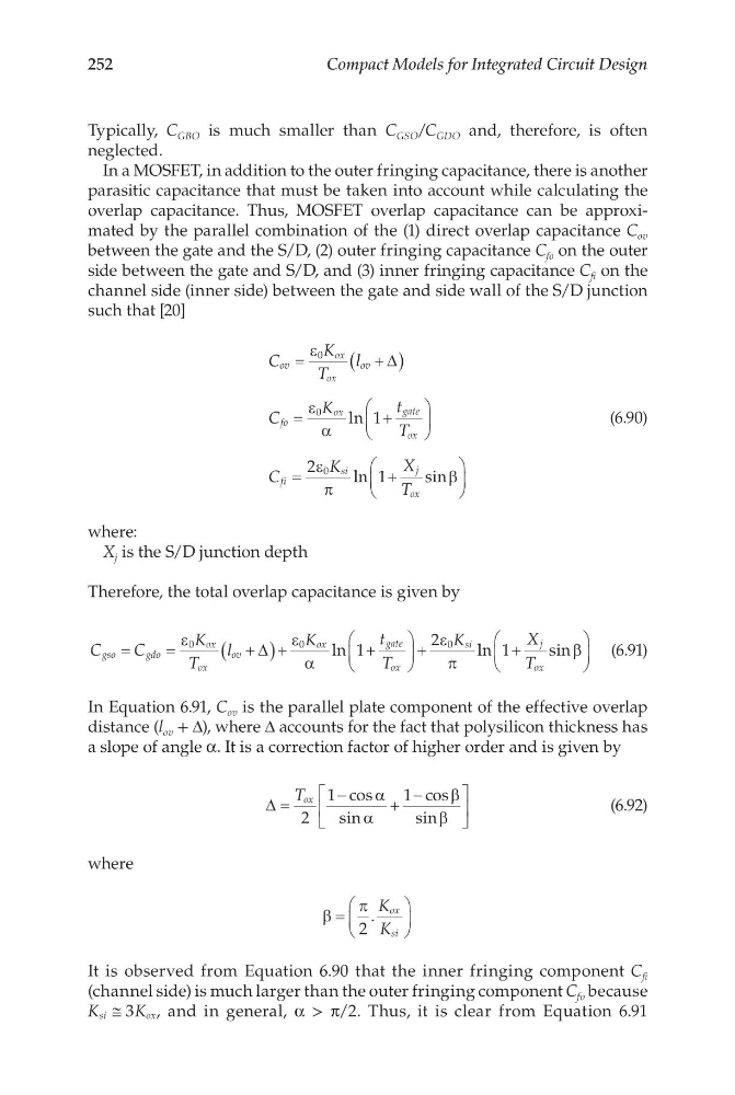
overlap capacitance. Thus, MOSFET overlap capacitance can be approximated by the parallel combination of the (1) direct overlap capacitance C ov
between the gate and the S/D, (2) outer fringing capacitance C fo on the outer
side between the gate and S/D, and (3) inner fringing capacitance C fi on the
channel side (inner side) between the gate and side wall of the S/D junction
such that [20]
C
K
T
l
C
K
t
T
C
K
ov
ox
ox
ov
fo
ox
gate
ox
fi
si
=
+
(
)
=
+
=
ε
ε
α
ε
π
0
0
0
1
2
∆
ln
l ln
sin
1+
X
T
j
ox
β
(6.90)
where:
X j is the S/D junction depth
Therefore, the total overlap capacitance is given by
C
C
K
T
l
K
t
T
K
gso
gdo
ox
ox
ov
ox
gate
ox
si
=
=
+
(
)+
+
+
ε
ε
α
ε
π
0
0
0
1
2
∆
ln
l ln
sin
1+
X
T
j
ox
β
(6.91)
In Equation 6.91, C ov is the parallel plate component of the effective overlap
distance (l ov + Δ), where Δ accounts for the fact that polysilicon thickness has
a slope of angle α. It is a correction factor of higher order and is given by
∆ =
−
+
−
T ox
2
1
1
cos
sin
cos
sin
α
α
β
β
(6.92)
where
β
π
=
2
.
K
K
ox
si
It is observed from Equation 6.90 that the inner fringing component C fi
(channel side) is much larger than the outer fringing component C fo because
K
K
si
ox
≅ 3 , and in general, α > π/2. Thus, it is clear from Equation 6.91
Compact Models for Integrated Circuit Design
Typically, C GBO is much smaller than C GSO /C GDO and, therefore, is often
neglected.
In a MOSFET, in addition to the outer fringing capacitance, there is another
parasitic capacitance that must be taken into account while calculating the
overlap capacitance. Thus, MOSFET overlap capacitance can be approximated by the parallel combination of the (1) direct overlap capacitance C ov
between the gate and the S/D, (2) outer fringing capacitance C fo on the outer
side between the gate and S/D, and (3) inner fringing capacitance C fi on the
channel side (inner side) between the gate and side wall of the S/D junction
such that [20]
C
K
T
l
C
K
t
T
C
K
ov
ox
ox
ov
fo
ox
gate
ox
fi
si
=
+
(
)
=
+
=
ε
ε
α
ε
π
0
0
0
1
2
∆
ln
l ln
sin
1+
X
T
j
ox
β
(6.90)
where:
X j is the S/D junction depth
Therefore, the total overlap capacitance is given by
C
C
K
T
l
K
t
T
K
gso
gdo
ox
ox
ov
ox
gate
ox
si
=
=
+
(
)+
+
+
ε
ε
α
ε
π
0
0
0
1
2
∆
ln
l ln
sin
1+
X
T
j
ox
β
(6.91)
In Equation 6.91, C ov is the parallel plate component of the effective overlap
distance (l ov + Δ), where Δ accounts for the fact that polysilicon thickness has
a slope of angle α. It is a correction factor of higher order and is given by
∆ =
−
+
−
T ox
2
1
1
cos
sin
cos
sin
α
α
β
β
(6.92)
where
β
π
=
2
.
K
K
ox
si
It is observed from Equation 6.90 that the inner fringing component C fi
(channel side) is much larger than the outer fringing component C fo because
K
K
si
ox
≅ 3 , and in general, α > π/2. Thus, it is clear from Equation 6.91