

251
MOSFET Capacitance Models
6.4 Gate Overlap Capacitance Model
The S/D overlap capacitances are parasitic elements that originate due to
the encroachment of S/D implant profile under the gate region during IC
(integrated circuit) fabrication processes. The postimplant thermal processing steps cause lateral diffusion of dopants under the gate and overlap of the
S/D regions in the final device structure. Since in MOSFETs, S/D regions
are normally symmetrical, the source overlap distance l ov is same as that of
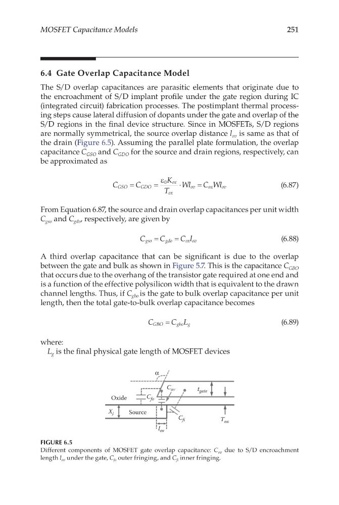
the drain (Figure 6.5). Assuming the parallel plate formulation, the overlap
capacitance C GSO and C GDO for the source and drain regions, respectively, can
be approximated as
C
C
K
T
Wl
C Wl
GSO
G DO
ox
ox
ov
ox
ov
=
=
⋅
=
ε 0
(6.87)
From Equation 6.87, the source and drain overlap capacitances per unit width
C gso and C gdo , respectively, are given by
C
C
C l
gso
gdo
ox ov
= =
(6.88)
A third overlap capacitance that can be significant is due to the overlap
between the gate and bulk as shown in Figure 5.7. This is the capacitance C GBO
that occurs due to the overhang of the transistor gate required at one end and
is a function of the effective polysilicon width that is equivalent to the drawn
channel lengths. Thus, if C gbo is the gate to bulk overlap capacitance per unit
length, then the total gate-to-bulk overlap capacitance becomes
C
C L
GBO
g bo g
=
(6.89)
where:
L g is the final physical gate length of MOSFET devices
Source
Oxide
X j
C fo
C ov
t gate
l ov
C fi
T ox
α
FIGURE 6.5
Different components of MOSFET gate overlap capacitance: C ov due to S/D encroachment
length l ov under the gate, C fo outer fringing, and C fi inner fringing.
MOSFET Capacitance Models
6.4 Gate Overlap Capacitance Model
The S/D overlap capacitances are parasitic elements that originate due to
the encroachment of S/D implant profile under the gate region during IC
(integrated circuit) fabrication processes. The postimplant thermal processing steps cause lateral diffusion of dopants under the gate and overlap of the
S/D regions in the final device structure. Since in MOSFETs, S/D regions
are normally symmetrical, the source overlap distance l ov is same as that of
the drain (Figure 6.5). Assuming the parallel plate formulation, the overlap
capacitance C GSO and C GDO for the source and drain regions, respectively, can
be approximated as
C
C
K
T
Wl
C Wl
GSO
G DO
ox
ox
ov
ox
ov
=
=
⋅
=
ε 0
(6.87)
From Equation 6.87, the source and drain overlap capacitances per unit width
C gso and C gdo , respectively, are given by
C
C
C l
gso
gdo
ox ov
= =
(6.88)
A third overlap capacitance that can be significant is due to the overlap
between the gate and bulk as shown in Figure 5.7. This is the capacitance C GBO
that occurs due to the overhang of the transistor gate required at one end and
is a function of the effective polysilicon width that is equivalent to the drawn
channel lengths. Thus, if C gbo is the gate to bulk overlap capacitance per unit
length, then the total gate-to-bulk overlap capacitance becomes
C
C L
GBO
g bo g
=
(6.89)
where:
L g is the final physical gate length of MOSFET devices
Source
Oxide
X j
C fo
C ov
t gate
l ov
C fi
T ox
α
FIGURE 6.5
Different components of MOSFET gate overlap capacitance: C ov due to S/D encroachment
length l ov under the gate, C fo outer fringing, and C fi inner fringing.