

256
Compact Models for Integrated Circuit Design
6.6 S/D pn-Junction Capacitance Model
Source-drain pn-junction capacitances consist of three components: the bottom junction capacitance, sidewall junction capacitance along the isolation
edge, and sidewall junction capacitance along the gate edge. An analogous
set of equations are used for both sides but each side has a separate set of
model parameters.
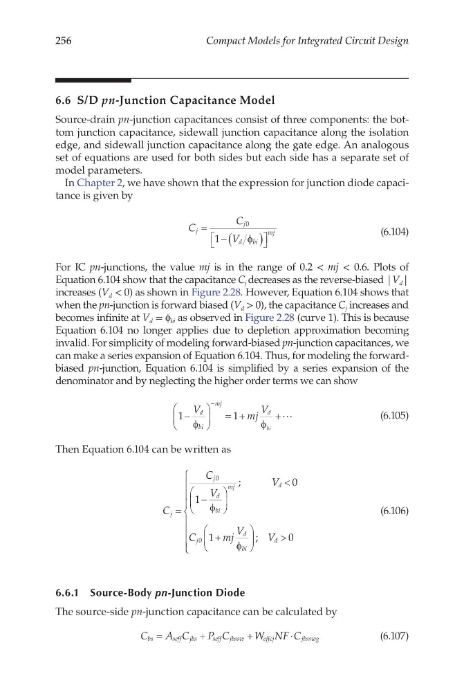
In Chapter 2, we have shown that the expression for junction diode capacitance is given by
C
C
V
j
j
d
bi
mj
=
− (
)
0
1
φ
(6.104)
For IC pn-junctions, the value mj is in the range of 0.2 < mj < 0.6. Plots of
Equ ation 6.104 show that the capacitance C j decreases as the reverse-biased |V d |
increases (V d < 0) as shown in Figure 2.28. However, Equation 6.104 shows that
when the pn-junction is forward biased (V d > 0), the capacitance C j increases and
becomes infinite at V d = f bi as observed in Figure 2.28 (curve 1). This is because
Equation 6.104 no longer applies due to depletion approximation becoming
invalid. For simplicity of modeling forward-biased pn-junction capacitances, we
can make a series expansion of Equation 6.104. Thus, for modeling the forwardbiased pn-junction, Equation 6.104 is simplified by a series expansion of the
denominator and by neglecting the higher order terms we can show
1
1
−
= +
+
−
V
mj
V
d
bi
mj
d
bi
φ
φ
(6.105)
Then Equation 6.104 can be written as
C
C
V
V
C
mj
V
V
j
j
d
bi
mj
d
j
d
bi
=
−
<
+
>
0
0
1
0
1
0
φ
φ
;
;
d
(6.106)
6.6.1 Source-Body pn-Junction Diode
The source-side pn-junction capacitance can be calculated by
C
A C
P C
W NF C
bs
seff jbs
seff jbssw
effcj
j bsswg
=
+
+
⋅
(6.107)
Compact Models for Integrated Circuit Design
6.6 S/D pn-Junction Capacitance Model
Source-drain pn-junction capacitances consist of three components: the bottom junction capacitance, sidewall junction capacitance along the isolation
edge, and sidewall junction capacitance along the gate edge. An analogous
set of equations are used for both sides but each side has a separate set of
model parameters.
In Chapter 2, we have shown that the expression for junction diode capacitance is given by
C
C
V
j
j
d
bi
mj
=
− (
)
0
1
φ
(6.104)
For IC pn-junctions, the value mj is in the range of 0.2 < mj < 0.6. Plots of
Equ ation 6.104 show that the capacitance C j decreases as the reverse-biased |V d |
increases (V d < 0) as shown in Figure 2.28. However, Equation 6.104 shows that
when the pn-junction is forward biased (V d > 0), the capacitance C j increases and
becomes infinite at V d = f bi as observed in Figure 2.28 (curve 1). This is because
Equation 6.104 no longer applies due to depletion approximation becoming
invalid. For simplicity of modeling forward-biased pn-junction capacitances, we
can make a series expansion of Equation 6.104. Thus, for modeling the forwardbiased pn-junction, Equation 6.104 is simplified by a series expansion of the
denominator and by neglecting the higher order terms we can show
1
1
−
= +
+
−
V
mj
V
d
bi
mj
d
bi
φ
φ
(6.105)
Then Equation 6.104 can be written as
C
C
V
V
C
mj
V
V
j
j
d
bi
mj
d
j
d
bi
=
−
<
+
>
0
0
1
0
1
0
φ
φ
;
;
d
(6.106)
6.6.1 Source-Body pn-Junction Diode
The source-side pn-junction capacitance can be calculated by
C
A C
P C
W NF C
bs
seff jbs
seff jbssw
effcj
j bsswg
=
+
+
⋅
(6.107)