

243
MOSFET Capacitance Models
When V ds = 0, it is found from Equations 6.54 and 6.55, Q S = Q D =
(1/2)WLC V V
ox
gs
th
(
)
−
, which is obvious because of the symmetry.
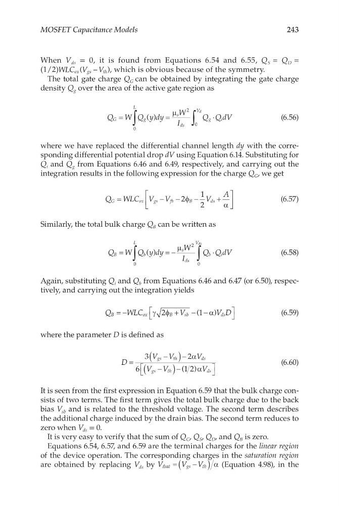
The total gate charge Q G can be obtained by integrating the gate charge
density Q g over the area of the active gate region as
Q W Q y dy
W
I
Q Q dV
G
g
L
s
ds
g
i
Vd
=
=
∫
∫
( )
0
2
0
µ
⋅
(6.56)
where we have replaced the differential channel length dy with the corresponding differential potential drop dV using Equation 6.14. Substituting for
Q i and Q g from Equations 6.46 and 6.49, respectively, and carrying out the
integration results in the following expression for the charge Q G , we get
Q WLC V V
V
A
G
o x
g s
f b
B
ds
=
−
−
−
+
2
1
2
φ
α
(6.57)
Similarly, the total bulk charge Q B can be written as
Q W Q y dy
W
I
Q Q dV
B
b
s
ds
L
b
i
Vds
=
= −
∫
∫
( )
µ
2
0
0
⋅
(6.58)
Again, substituting Q i and Q b from Equations 6.46 and 6.47 (or 6.50), respectively, and carrying out the integration yields
Q
WLC
V
V D
B
o x
B
sb
ds
= −
+
− −
γ φ
α
2
1
(
)
(6.59)
where the parameter D is defined as
D
V V
V
V V
V
gs
th
ds
gs
th
ds
=
−
(
) −
−
(
) −
3
2
6
12
α
α
( )
(6.60)
It is seen from the first expression in Equation 6.59 that the bulk charge consists of two terms. The first term gives the total bulk charge due to the back
bias V sb and is related to the threshold voltage. The second term describes
the additional charge induced by the drain bias. The second term reduces to
zero when V ds = 0.
It is very easy to verify that the sum of Q G , Q S , Q D , and Q B is zero.
Equations 6.54, 6.57, and 6.59 are the terminal charges for the linear region
of the device operation. The corresponding charges in the saturation region
are obtained by replacing V ds by V
V V
dsat
gs
th
=
−
(
) α (Equation 4.98), in the
MOSFET Capacitance Models
When V ds = 0, it is found from Equations 6.54 and 6.55, Q S = Q D =
(1/2)WLC V V
ox
gs
th
(
)
−
, which is obvious because of the symmetry.
The total gate charge Q G can be obtained by integrating the gate charge
density Q g over the area of the active gate region as
Q W Q y dy
W
I
Q Q dV
G
g
L
s
ds
g
i
Vd
=
=
∫
∫
( )
0
2
0
µ
⋅
(6.56)
where we have replaced the differential channel length dy with the corresponding differential potential drop dV using Equation 6.14. Substituting for
Q i and Q g from Equations 6.46 and 6.49, respectively, and carrying out the
integration results in the following expression for the charge Q G , we get
Q WLC V V
V
A
G
o x
g s
f b
B
ds
=
−
−
−
+
2
1
2
φ
α
(6.57)
Similarly, the total bulk charge Q B can be written as
Q W Q y dy
W
I
Q Q dV
B
b
s
ds
L
b
i
Vds
=
= −
∫
∫
( )
µ
2
0
0
⋅
(6.58)
Again, substituting Q i and Q b from Equations 6.46 and 6.47 (or 6.50), respectively, and carrying out the integration yields
Q
WLC
V
V D
B
o x
B
sb
ds
= −
+
− −
γ φ
α
2
1
(
)
(6.59)
where the parameter D is defined as
D
V V
V
V V
V
gs
th
ds
gs
th
ds
=
−
(
) −
−
(
) −
3
2
6
12
α
α
( )
(6.60)
It is seen from the first expression in Equation 6.59 that the bulk charge consists of two terms. The first term gives the total bulk charge due to the back
bias V sb and is related to the threshold voltage. The second term describes
the additional charge induced by the drain bias. The second term reduces to
zero when V ds = 0.
It is very easy to verify that the sum of Q G , Q S , Q D , and Q B is zero.
Equations 6.54, 6.57, and 6.59 are the terminal charges for the linear region
of the device operation. The corresponding charges in the saturation region
are obtained by replacing V ds by V
V V
dsat
gs
th
=
−
(
) α (Equation 4.98), in the