

235
MOSFET Capacitance Models
At V gs = V fb , the calculated value of C GB from Equation 6.27 is not accurate due
to the failure of the depletion approximation used in deriving Equation 6.27.
However, because of the simplicity of calculation, Equation 6.27 is used for
computing C GB at weak inversion.
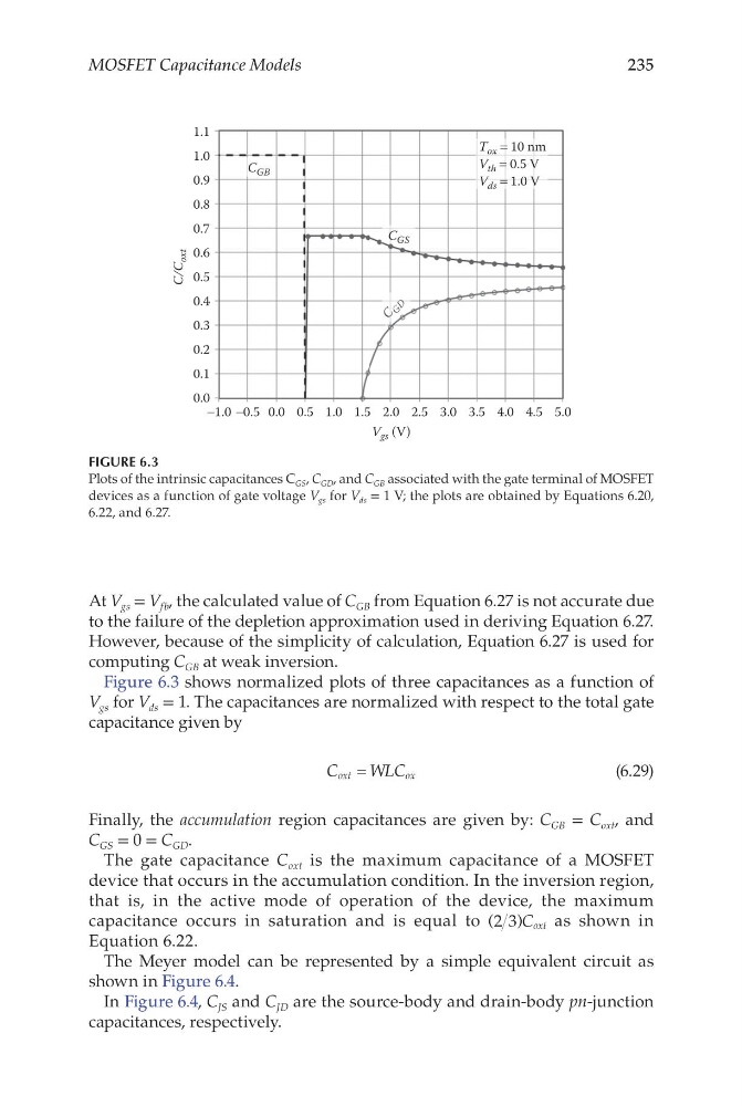
Figure 6.3 shows normalized plots of three capacitances as a function of
V gs for V ds = 1. The capacitances are normalized with respect to the total gate
capacitance given by
C
WLC
oxt
o x
=
(6.29)
Finally, the accumulation region capacitances are given by: C GB = C oxt , and
C GS = 0 = C GD .
The gate capacitance C oxt is the maximum capacitance of a MOSFET
device that occurs in the accumulation condition. In the inversion region,
that is, in the active mode of operation of the device, the maximum
capacitance occurs in saturation and is equal to ( )
2 3 C oxt as shown in
Equation 6.22.
The Meyer model can be represented by a simple equivalent circuit as
shown in Figure 6.4.
In Figure 6.4, C JS and C JD are the source-body and drain-body pn-junction
capacitances, respectively.
0.0
−1.0 −0.5 0.0 0.5 1.0 1.5 2.0
V gs (V)
C
G D
T ox = 10 nm
C/C
oxt
V th = 0.5 V
V ds = 1.0 V
2.5 3.0 3.5 4.0 4.5 5.0
0.1
0.2
0.3
0.4
0.5
0.6
0.7
0.8
0.9
1.0
1.1
C GS
C GB
FIGURE 6.3
Plots of the intrinsic capacitances C GS , C GD , and C GB associated with the gate terminal of MOSFET
devices as a function of gate voltage V gs for V ds = 1 V; the plots are obtained by Equations 6.20,
6.22, and 6.27.
MOSFET Capacitance Models
At V gs = V fb , the calculated value of C GB from Equation 6.27 is not accurate due
to the failure of the depletion approximation used in deriving Equation 6.27.
However, because of the simplicity of calculation, Equation 6.27 is used for
computing C GB at weak inversion.
Figure 6.3 shows normalized plots of three capacitances as a function of
V gs for V ds = 1. The capacitances are normalized with respect to the total gate
capacitance given by
C
WLC
oxt
o x
=
(6.29)
Finally, the accumulation region capacitances are given by: C GB = C oxt , and
C GS = 0 = C GD .
The gate capacitance C oxt is the maximum capacitance of a MOSFET
device that occurs in the accumulation condition. In the inversion region,
that is, in the active mode of operation of the device, the maximum
capacitance occurs in saturation and is equal to ( )
2 3 C oxt as shown in
Equation 6.22.
The Meyer model can be represented by a simple equivalent circuit as
shown in Figure 6.4.
In Figure 6.4, C JS and C JD are the source-body and drain-body pn-junction
capacitances, respectively.
0.0
−1.0 −0.5 0.0 0.5 1.0 1.5 2.0
V gs (V)
C
G D
T ox = 10 nm
C/C
oxt
V th = 0.5 V
V ds = 1.0 V
2.5 3.0 3.5 4.0 4.5 5.0
0.1
0.2
0.3
0.4
0.5
0.6
0.7
0.8
0.9
1.0
1.1
C GS
C GB
FIGURE 6.3
Plots of the intrinsic capacitances C GS , C GD , and C GB associated with the gate terminal of MOSFET
devices as a function of gate voltage V gs for V ds = 1 V; the plots are obtained by Equations 6.20,
6.22, and 6.27.