

234
Compact Models for Integrated Circuit Design
6.2.2.2 Weak Inversion
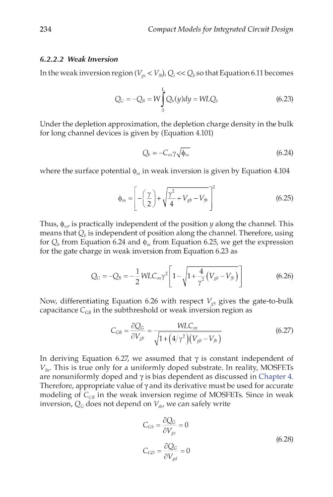
In the weak inversion region (V gs < V th ), Q i << Q b so that Equation 6.11 becomes
Q
Q W Q y dy WLQ
G
B
b
L
b
= − =
=
∫
( )
0
(6.23)
Under the depletion approximation, the depletion charge density in the bulk
for long channel devices is given by (Equation 4.101)
Q
C
b
o x
s s
= − γ φ
(6.24)
where the surface potential f ss in weak inversion is given by Equation 4.104
φ
γ
γ
ss
gb
fb
V V
= −
+
+
−
2
4
2
2
(6.25)
Thus, f ss , is practically independent of the position y along the channel. This
means that Q b is independent of position along the channel. Therefore, using
for Q b from Equation 6.24 and f ss from Equation 6.25, we get the expression
for the gate charge in weak inversion from Equation 6.23 as
Q
Q
WLC
V V
G
B
ox
gb
fb
= − = −
− +
−
(
)
1
2
1 1
4
2
2
γ
γ
(6.26)
Now, differentiating Equation 6.26 with respect V gb gives the gate-to-bulk
capacitance C GB in the subthreshold or weak inversion region as
C
Q
V
WLC
V V
GB
G
gb
ox
gb
fb
=
∂
∂
=
+ ( ) −
(
)
1 4
2
γ
(6.27)
In deriving Equation 6.27, we assumed that γ is constant independent of
V bs . This is true only for a uniformly doped substrate. In reality, MOSFETs
are nonuniformly doped and γ is bias dependent as discussed in Chapter 4.
Therefore, appropriate value of γ and its derivative must be used for accurate
modeling of C GB in the weak inversion regime of MOSFETs. Since in weak
inversion, Q G does not depend on V ds , we can safely write
C
Q
V
C
Q
V
GS
G
gs
GD
G
gd
=
∂
∂
=
=
∂
∂
=
0
0
(6.28)
Compact Models for Integrated Circuit Design
6.2.2.2 Weak Inversion
In the weak inversion region (V gs < V th ), Q i << Q b so that Equation 6.11 becomes
Q
Q W Q y dy WLQ
G
B
b
L
b
= − =
=
∫
( )
0
(6.23)
Under the depletion approximation, the depletion charge density in the bulk
for long channel devices is given by (Equation 4.101)
Q
C
b
o x
s s
= − γ φ
(6.24)
where the surface potential f ss in weak inversion is given by Equation 4.104
φ
γ
γ
ss
gb
fb
V V
= −
+
+
−
2
4
2
2
(6.25)
Thus, f ss , is practically independent of the position y along the channel. This
means that Q b is independent of position along the channel. Therefore, using
for Q b from Equation 6.24 and f ss from Equation 6.25, we get the expression
for the gate charge in weak inversion from Equation 6.23 as
Q
Q
WLC
V V
G
B
ox
gb
fb
= − = −
− +
−
(
)
1
2
1 1
4
2
2
γ
γ
(6.26)
Now, differentiating Equation 6.26 with respect V gb gives the gate-to-bulk
capacitance C GB in the subthreshold or weak inversion region as
C
Q
V
WLC
V V
GB
G
gb
ox
gb
fb
=
∂
∂
=
+ ( ) −
(
)
1 4
2
γ
(6.27)
In deriving Equation 6.27, we assumed that γ is constant independent of
V bs . This is true only for a uniformly doped substrate. In reality, MOSFETs
are nonuniformly doped and γ is bias dependent as discussed in Chapter 4.
Therefore, appropriate value of γ and its derivative must be used for accurate
modeling of C GB in the weak inversion regime of MOSFETs. Since in weak
inversion, Q G does not depend on V ds , we can safely write
C
Q
V
C
Q
V
GS
G
gs
GD
G
gd
=
∂
∂
=
=
∂
∂
=
0
0
(6.28)