

230
Compact Models for Integrated Circuit Design
bulk (C GB ). These are defined as the derivative of the total gate charge Q G with
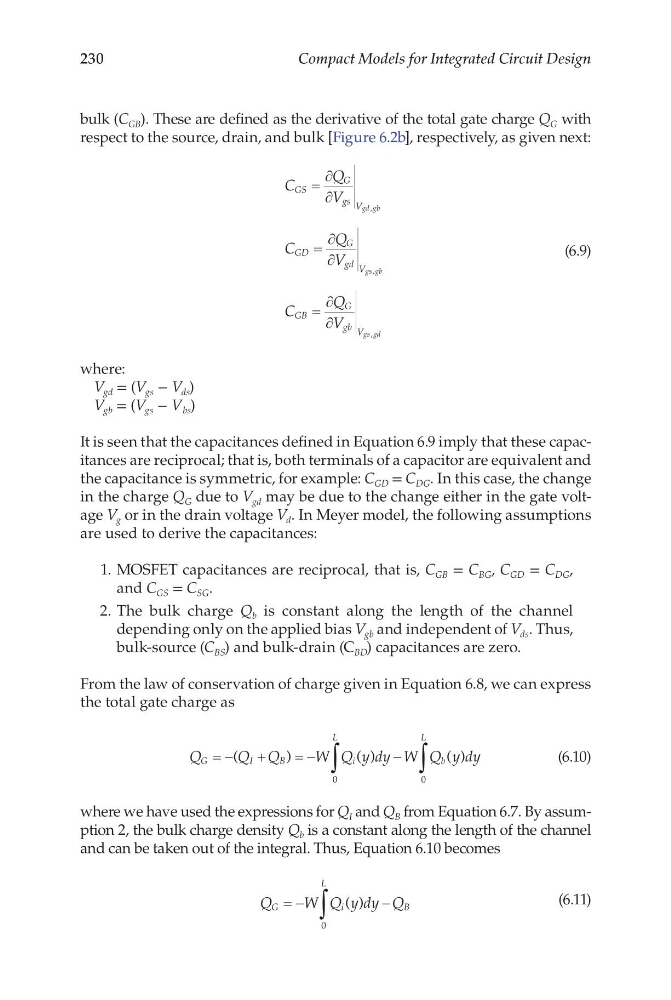
respect to the source, drain, and bulk [Figure 6.2b], respectively, as given next:
C
Q
V
C
Q
V
C
Q
V
GS
G
gs V
GD
G
gd V
GB
G
gb V
gd gb
gs gb
gs gd
=
∂
∂
=
∂
∂
=
∂
∂
,
,
,
(6.9)
where:
V gd = (V gs − V ds )
V gb = (V gs − V bs )
It is seen that the capacitances defined in Equation 6.9 imply that these capacitances are reciprocal; that is, both terminals of a capacitor are equivalent and
the capacitance is symmetric, for example: C GD = C DG . In this case, the change
in the charge Q G due to V gd may be due to the change either in the gate voltage V g or in the drain voltage V d . In Meyer model, the following assumptions
are used to derive the capacitances:
1. MOSFET capacitances are reciprocal, that is, C GB = C BG , C GD = C DG ,
and C GS = C SG .
2. The bulk charge Q b is constant along the length of the channel
depending only on the applied bias V gb and independent of V ds . Thus,
bulk-source (C BS ) and bulk-drain (C BD ) capacitances are zero.
From the law of conservation of charge given in Equation 6.8, we can express
the total gate charge as
Q
Q Q
W Q y dy W Q y dy
G
I
B
i
L
b
L
= −
+
=−
−
∫
∫
(
)
( )
( )
0
0
(6.10)
where we have used the expressions for Q I and Q B from Equation 6.7. By assumption 2, the bulk charge density Q b is a constant along the length of the channel
and can be taken out of the integral. Thus, Equation 6.10 becomes
Q
W Q y dy Q
G
i
L
B
= −
−
∫
( )
0
(6.11)
Compact Models for Integrated Circuit Design
bulk (C GB ). These are defined as the derivative of the total gate charge Q G with
respect to the source, drain, and bulk [Figure 6.2b], respectively, as given next:
C
Q
V
C
Q
V
C
Q
V
GS
G
gs V
GD
G
gd V
GB
G
gb V
gd gb
gs gb
gs gd
=
∂
∂
=
∂
∂
=
∂
∂
,
,
,
(6.9)
where:
V gd = (V gs − V ds )
V gb = (V gs − V bs )
It is seen that the capacitances defined in Equation 6.9 imply that these capacitances are reciprocal; that is, both terminals of a capacitor are equivalent and
the capacitance is symmetric, for example: C GD = C DG . In this case, the change
in the charge Q G due to V gd may be due to the change either in the gate voltage V g or in the drain voltage V d . In Meyer model, the following assumptions
are used to derive the capacitances:
1. MOSFET capacitances are reciprocal, that is, C GB = C BG , C GD = C DG ,
and C GS = C SG .
2. The bulk charge Q b is constant along the length of the channel
depending only on the applied bias V gb and independent of V ds . Thus,
bulk-source (C BS ) and bulk-drain (C BD ) capacitances are zero.
From the law of conservation of charge given in Equation 6.8, we can express
the total gate charge as
Q
Q Q
W Q y dy W Q y dy
G
I
B
i
L
b
L
= −
+
=−
−
∫
∫
(
)
( )
( )
0
0
(6.10)
where we have used the expressions for Q I and Q B from Equation 6.7. By assumption 2, the bulk charge density Q b is a constant along the length of the channel
and can be taken out of the integral. Thus, Equation 6.10 becomes
Q
W Q y dy Q
G
i
L
B
= −
−
∫
( )
0
(6.11)