

229
MOSFET Capacitance Models
Q W Q y dy
G
g
L
=
∫
( )
0
(6.6)
Similarly, we can show
Q W Q y dy
Q W Q y dy
I
i
L
B
b
L
=
=
∫
∫
( )
( )
0
0
(6.7)
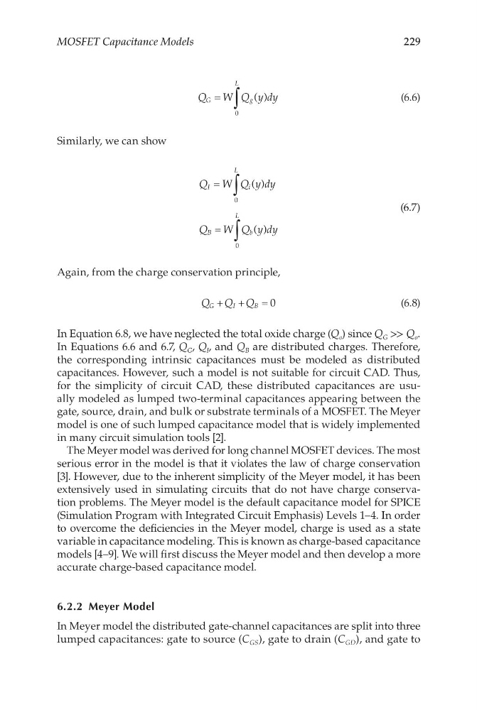
Again, from the charge conservation principle,
Q Q Q
G
I
B
+ +
= 0
(6.8)
In Equation 6.8, we have neglected the total oxide charge (Q o ) since Q G >> Q o .
In Equations 6.6 and 6.7, Q G , Q I , and Q B are distributed charges. Therefore,
the corresponding intrinsic capacitances must be modeled as distributed
capacitances. However, such a model is not suitable for circuit CAD. Thus,
for the simplicity of circuit CAD, these distributed capacitances are usually modeled as lumped two-terminal capacitances appearing between the
gate, source, drain, and bulk or substrate terminals of a MOSFET. The Meyer
model is one of such lumped capacitance model that is widely implemented
in many circuit simulation tools [2].
The Meyer model was derived for long channel MOSFET devices. The most
serious error in the model is that it violates the law of charge conservation
[3]. However, due to the inherent simplicity of the Meyer model, it has been
extensively used in simulating circuits that do not have charge conservation problems. The Meyer model is the default capacitance model for SPICE
(Simulation Program with Integrated Circuit Emphasis) Levels 1–4. In order
to overcome the deficiencies in the Meyer model, charge is used as a state
variable in capacitance modeling. This is known as charge-based capacitance
models [4–9]. We will first discuss the Meyer model and then develop a more
accurate charge-based capacitance model.
6.2.2 Meyer Model
In Meyer model the distributed gate-channel capacitances are split into three
lumped capacitances: gate to source (C GS ), gate to drain (C GD ), and gate to
MOSFET Capacitance Models
Q W Q y dy
G
g
L
=
∫
( )
0
(6.6)
Similarly, we can show
Q W Q y dy
Q W Q y dy
I
i
L
B
b
L
=
=
∫
∫
( )
( )
0
0
(6.7)
Again, from the charge conservation principle,
Q Q Q
G
I
B
+ +
= 0
(6.8)
In Equation 6.8, we have neglected the total oxide charge (Q o ) since Q G >> Q o .
In Equations 6.6 and 6.7, Q G , Q I , and Q B are distributed charges. Therefore,
the corresponding intrinsic capacitances must be modeled as distributed
capacitances. However, such a model is not suitable for circuit CAD. Thus,
for the simplicity of circuit CAD, these distributed capacitances are usually modeled as lumped two-terminal capacitances appearing between the
gate, source, drain, and bulk or substrate terminals of a MOSFET. The Meyer
model is one of such lumped capacitance model that is widely implemented
in many circuit simulation tools [2].
The Meyer model was derived for long channel MOSFET devices. The most
serious error in the model is that it violates the law of charge conservation
[3]. However, due to the inherent simplicity of the Meyer model, it has been
extensively used in simulating circuits that do not have charge conservation problems. The Meyer model is the default capacitance model for SPICE
(Simulation Program with Integrated Circuit Emphasis) Levels 1–4. In order
to overcome the deficiencies in the Meyer model, charge is used as a state
variable in capacitance modeling. This is known as charge-based capacitance
models [4–9]. We will first discuss the Meyer model and then develop a more
accurate charge-based capacitance model.
6.2.2 Meyer Model
In Meyer model the distributed gate-channel capacitances are split into three
lumped capacitances: gate to source (C GS ), gate to drain (C GD ), and gate to