

219
Compact Models for Small Geometry MOSFETs
I
NF AGIDL W
V V
EGIDL
TOXE
TOXE BG
gidl
eff
ds
gseff
=
−
−
−
.
.
exp
.
3
3
I IDL
V V
EGIDL
V
CGIDL V
I
NF AGIS
ds
gseff
DB
DB
gisl
−
−
+
=
3
3
and
.
L LW
V V
EGISL
TOXE
TOXE BGISL
V V
eff
ds
gseff
ds
gs
.
e xp
.
− −
−
−
− −
3
3
e eff
SB
SB
EGISL
V
CGISL V
−
+
3
3
(5.129)
The model parameters (AGIDL, AGISL), (BGIDL, BGISL), (CGIDL, CGISL),
and (EGIDL, EGISL) are obtained from the measured I ds − V gs data obtained
for −V gs to +V gs at V ds = V dd (supply voltage); NF is the number of fingers used
in the layout for MOSFETs. GIDL must be accounted if the standby current
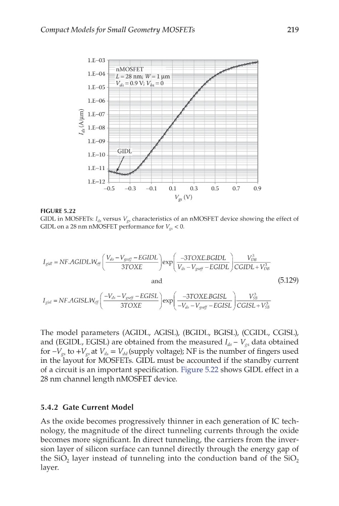
of a circuit is an important specification. Figure 5.22 shows GIDL effect in a
28 nm channel length nMOSFET device.
5.4.2 Gate Current Model
As the oxide becomes progressively thinner in each generation of IC technology, the magnitude of the direct tunneling currents through the oxide
becomes more significant. In direct tunneling, the carriers from the inversion layer of silicon surface can tunnel directly through the energy gap of
the SiO 2 layer instead of tunneling into the conduction band of the SiO 2
layer.
−0.5
1.E−12
1.E−11
1.E−10
1.E−09
1.E−08
1.E−07
1.E−06
1.E−05
1.E−04
1.E−03
−0.3
GIDL
nMOSFET
L = 28 nm; W = 1 μm
V ds = 0.9 V; V bs = 0
−0.1
0.1
V gs (V)
0.3
0.5
0.7
0.9
I
ds (A/μm)
FIGURE 5.22
GIDL in MOSFETs: I ds versus V gs characteristics of an nMOSFET device showing the effect of
GIDL on a 28 nm nMOSFET performance for V gs < 0.
Compact Models for Small Geometry MOSFETs
I
NF AGIDL W
V V
EGIDL
TOXE
TOXE BG
gidl
eff
ds
gseff
=
−
−
−
.
.
exp
.
3
3
I IDL
V V
EGIDL
V
CGIDL V
I
NF AGIS
ds
gseff
DB
DB
gisl
−
−
+
=
3
3
and
.
L LW
V V
EGISL
TOXE
TOXE BGISL
V V
eff
ds
gseff
ds
gs
.
e xp
.
− −
−
−
− −
3
3
e eff
SB
SB
EGISL
V
CGISL V
−
+
3
3
(5.129)
The model parameters (AGIDL, AGISL), (BGIDL, BGISL), (CGIDL, CGISL),
and (EGIDL, EGISL) are obtained from the measured I ds − V gs data obtained
for −V gs to +V gs at V ds = V dd (supply voltage); NF is the number of fingers used
in the layout for MOSFETs. GIDL must be accounted if the standby current
of a circuit is an important specification. Figure 5.22 shows GIDL effect in a
28 nm channel length nMOSFET device.
5.4.2 Gate Current Model
As the oxide becomes progressively thinner in each generation of IC technology, the magnitude of the direct tunneling currents through the oxide
becomes more significant. In direct tunneling, the carriers from the inversion layer of silicon surface can tunnel directly through the energy gap of
the SiO 2 layer instead of tunneling into the conduction band of the SiO 2
layer.
−0.5
1.E−12
1.E−11
1.E−10
1.E−09
1.E−08
1.E−07
1.E−06
1.E−05
1.E−04
1.E−03
−0.3
GIDL
nMOSFET
L = 28 nm; W = 1 μm
V ds = 0.9 V; V bs = 0
−0.1
0.1
V gs (V)
0.3
0.5
0.7
0.9
I
ds (A/μm)
FIGURE 5.22
GIDL in MOSFETs: I ds versus V gs characteristics of an nMOSFET device showing the effect of
GIDL on a 28 nm nMOSFET performance for V gs < 0.