

218
Compact Models for Integrated Circuit Design
5.4.1 Gate-Induced Drain Leakage Body Current Model
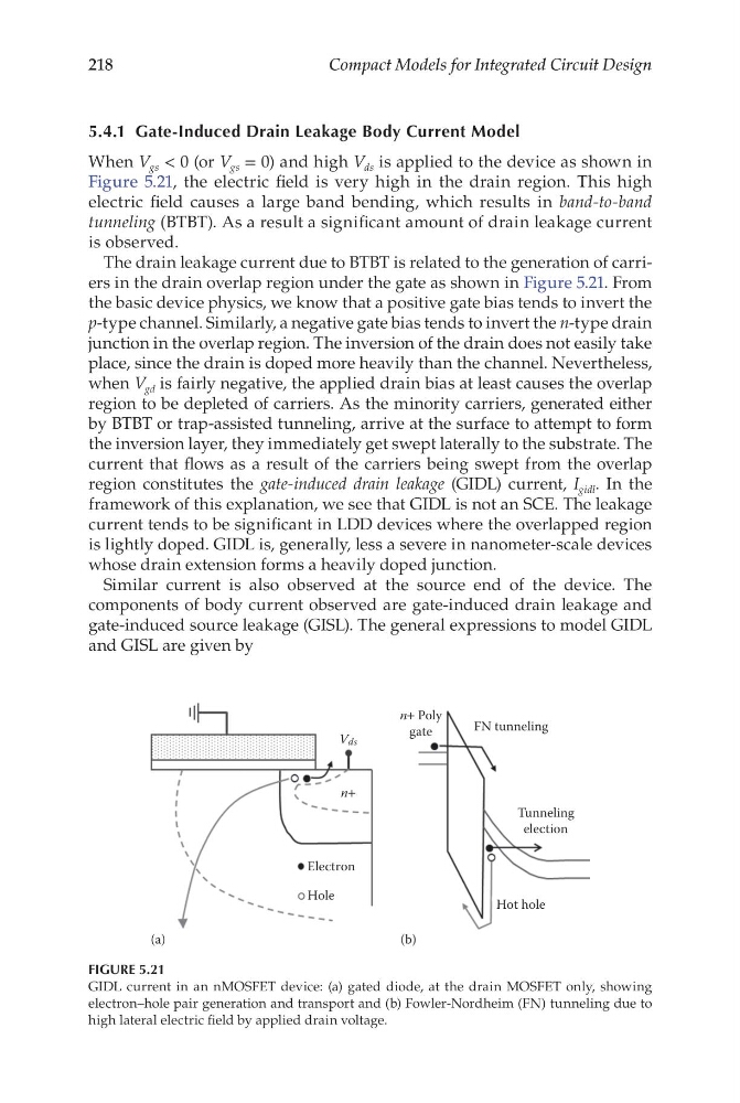
When V gs < 0 (or V gs = 0) and high V ds is applied to the device as shown in
Figure 5.21, the electric field is very high in the drain region. This high
electric field causes a large band bending, which results in band-to-band
tunneling (BTBT). As a result a significant amount of drain leakage current
is observed.
The drain leakage current due to BTBT is related to the generation of carriers in the drain overlap region under the gate as shown in Figure 5.21. From
the basic device physics, we know that a positive gate bias tends to invert the
p-type channel. Similarly, a negative gate bias tends to invert the n-type drain
junction in the overlap region. The inversion of the drain does not easily take
place, since the drain is doped more heavily than the channel. Nevertheless,
when V gd is fairly negative, the applied drain bias at least causes the overlap
region to be depleted of carriers. As the minority carriers, generated either
by BTBT or trap-assisted tunneling, arrive at the surface to attempt to form
the inversion layer, they immediately get swept laterally to the substrate. The
current that flows as a result of the carriers being swept from the overlap
region constitutes the gate-induced drain leakage (GIDL) current, I gidl . In the
framework of this explanation, we see that GIDL is not an SCE. The leakage
current tends to be significant in LDD devices where the overlapped region
is lightly doped. GIDL is, generally, less a severe in nanometer-scale devices
whose drain extension forms a heavily doped junction.
Similar current is also observed at the source end of the device. The
components of body current observed are gate-induced drain leakage and
gate-induced source leakage (GISL). The general expressions to model GIDL
and GISL are given by
Vds
n+
Electron
Hole
(a)
n+ Poly
gate
FN tunneling
Tunneling
election
Hot hole
(b)
FIGURE 5.21
GIDL current in an nMOSFET device: (a) gated diode, at the drain MOSFET only, showing
electron–hole pair generation and transport and (b) Fowler-Nordheim (FN) tunneling due to
high lateral electric field by applied drain voltage.
Compact Models for Integrated Circuit Design
5.4.1 Gate-Induced Drain Leakage Body Current Model
When V gs < 0 (or V gs = 0) and high V ds is applied to the device as shown in
Figure 5.21, the electric field is very high in the drain region. This high
electric field causes a large band bending, which results in band-to-band
tunneling (BTBT). As a result a significant amount of drain leakage current
is observed.
The drain leakage current due to BTBT is related to the generation of carriers in the drain overlap region under the gate as shown in Figure 5.21. From
the basic device physics, we know that a positive gate bias tends to invert the
p-type channel. Similarly, a negative gate bias tends to invert the n-type drain
junction in the overlap region. The inversion of the drain does not easily take
place, since the drain is doped more heavily than the channel. Nevertheless,
when V gd is fairly negative, the applied drain bias at least causes the overlap
region to be depleted of carriers. As the minority carriers, generated either
by BTBT or trap-assisted tunneling, arrive at the surface to attempt to form
the inversion layer, they immediately get swept laterally to the substrate. The
current that flows as a result of the carriers being swept from the overlap
region constitutes the gate-induced drain leakage (GIDL) current, I gidl . In the
framework of this explanation, we see that GIDL is not an SCE. The leakage
current tends to be significant in LDD devices where the overlapped region
is lightly doped. GIDL is, generally, less a severe in nanometer-scale devices
whose drain extension forms a heavily doped junction.
Similar current is also observed at the source end of the device. The
components of body current observed are gate-induced drain leakage and
gate-induced source leakage (GISL). The general expressions to model GIDL
and GISL are given by
Vds
n+
Electron
Hole
(a)
n+ Poly
gate
FN tunneling
Tunneling
election
Hot hole
(b)
FIGURE 5.21
GIDL current in an nMOSFET device: (a) gated diode, at the drain MOSFET only, showing
electron–hole pair generation and transport and (b) Fowler-Nordheim (FN) tunneling due to
high lateral electric field by applied drain voltage.