

220
Compact Models for Integrated Circuit Design
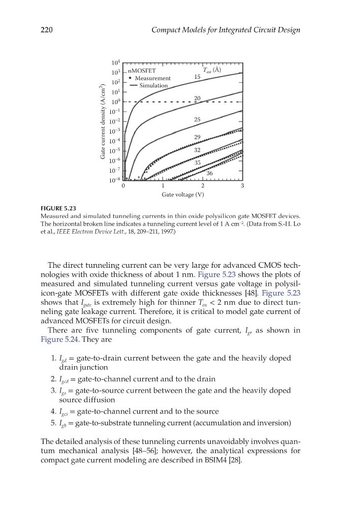
The direct tunneling current can be very large for advanced CMOS technologies with oxide thickness of about 1 nm. Figure 5.23 shows the plots of
measured and simulated tunneling current versus gate voltage in polysilicon-gate MOSFETs with different gate oxide thicknesses [48]. Figure 5.23
shows that I gate is extremely high for thinner T ox < 2 nm due to direct tunneling gate leakage current. Therefore, it is critical to model gate current of
advanced MOSFETs for circuit design.
There are five tunneling components of gate current, I g , as shown in
Figure 5.24. They are
1. I gd = gate-to-drain current between the gate and the heavily doped
drain junction
2. I gcd = gate-to-channel current and to the drain
3. I gs = gate-to-source current between the gate and the heavily doped
source diffusion
4. I gcs = gate-to-channel current and to the source
5. I gb = gate-to-substrate tunneling current (accumulation and inversion)
The detailed analysis of these tunneling currents unavoidably involves quantum mechanical analysis [48–56]; however, the analytical expressions for
compact gate current modeling are described in BSIM4 [28].
0
10
−8
10
−7
10
−6
10 −5
10
−4
10
−3
10
−2
10
−1
10
0
10
1
10
2
10
3
10
4
1
2
36
35
32
29
25
20
15
nMOSFET
T ox (Å)
Measurement
Simulation
Gate current density (A/cm
2
)
Gate voltage (V)
3
FIGURE 5.23
Measured and simulated tunneling currents in thin oxide polysilicon gate MOSFET devices.
The horizontal broken line indicates a tunneling current level of 1 A cm −2 . (Data from S.-H. Lo
et al., IEEE Electron Device Lett., 18, 209–211, 1997.)
Compact Models for Integrated Circuit Design
The direct tunneling current can be very large for advanced CMOS technologies with oxide thickness of about 1 nm. Figure 5.23 shows the plots of
measured and simulated tunneling current versus gate voltage in polysilicon-gate MOSFETs with different gate oxide thicknesses [48]. Figure 5.23
shows that I gate is extremely high for thinner T ox < 2 nm due to direct tunneling gate leakage current. Therefore, it is critical to model gate current of
advanced MOSFETs for circuit design.
There are five tunneling components of gate current, I g , as shown in
Figure 5.24. They are
1. I gd = gate-to-drain current between the gate and the heavily doped
drain junction
2. I gcd = gate-to-channel current and to the drain
3. I gs = gate-to-source current between the gate and the heavily doped
source diffusion
4. I gcs = gate-to-channel current and to the source
5. I gb = gate-to-substrate tunneling current (accumulation and inversion)
The detailed analysis of these tunneling currents unavoidably involves quantum mechanical analysis [48–56]; however, the analytical expressions for
compact gate current modeling are described in BSIM4 [28].
0
10
−8
10
−7
10
−6
10 −5
10
−4
10
−3
10
−2
10
−1
10
0
10
1
10
2
10
3
10
4
1
2
36
35
32
29
25
20
15
nMOSFET
T ox (Å)
Measurement
Simulation
Gate current density (A/cm
2
)
Gate voltage (V)
3
FIGURE 5.23
Measured and simulated tunneling currents in thin oxide polysilicon gate MOSFET devices.
The horizontal broken line indicates a tunneling current level of 1 A cm −2 . (Data from S.-H. Lo
et al., IEEE Electron Device Lett., 18, 209–211, 1997.)