

205
Compact Models for Small Geometry MOSFETs
I
I
R I V
C
V
V
V
ds
ds
ds ds
dseff
l m
A
Asat
ds
= + (
)
+
+
0
0
1
1
1
1
ln
.
− −
+
−
+
−
V
V
V V
V
V V
dseff
ADIBL
ds
dseff
ASCBE
ds
dseff
.
.
1
1
V V ADITS
(5.87)
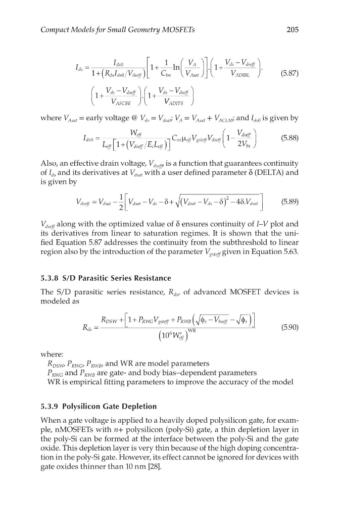
where V Asat = early voltage @ V ds = V dsat ; V A = V Asat + V ACLM ; and I ds0 is given by
I
W
L
V
E L
C
V V
V
ds
eff
eff
d seff
c eff
ox eff gsteff dseff
ds
0
1
1
=
+ (
)
−
µ
e eff
bs
V
2
(5.88)
Also, an effective drain voltage, V dseff , is a function that guarantees continuity
of I ds and its derivatives at V dsat with a user defined parameter δ (DELTA) and
is given by
V
V
V
V
V
V
V
dseff
d sat
d sat
d s
d sat
d s
d sat
=
−
−
− +
−
−
(
)−
1
2
4
2
δ
δ
δ.
(5.89)
V dseff along with the optimized value of δ ensures continuity of I–V plot and
its derivatives from linear to saturation regimes. It is shown that the unified Equation 5.87 addresses the continuity from the subthreshold to linear
region also by the introduction of the parameter V gsteff given in Equation 5.63.
5.3.8 S/D Parasitic Series Resistance
The S/D parasitic series resistance, R ds , of advanced MOSFET devices is
modeled as
R
R
P V
P
V
W
ds
DSW
R WG gsteff
RWB
s
bseff
s
eff
=
+ +
+
−
−
(
)
′
(
)
1
10
6
φ
φ
WR
(5.90)
where:
R DSW , P RWG , P RWB , and WR are model parameters
P RWG and P RWB are gate- and body bias–dependent parameters
WR is empirical fitting parameters to improve the accuracy of the model
5.3.9 Polysilicon Gate Depletion
When a gate voltage is applied to a heavily doped polysilicon gate, for example, nMOSFETs with n+ polysilicon (poly-Si) gate, a thin depletion layer in
the poly-Si can be formed at the interface between the poly-Si and the gate
oxide. This depletion layer is very thin because of the high doping concentration in the poly-Si gate. However, its effect cannot be ignored for devices with
gate oxides thinner than 10 nm [28].
Compact Models for Small Geometry MOSFETs
I
I
R I V
C
V
V
V
ds
ds
ds ds
dseff
l m
A
Asat
ds
= + (
)
+
+
0
0
1
1
1
1
ln
.
− −
+
−
+
−
V
V
V V
V
V V
dseff
ADIBL
ds
dseff
ASCBE
ds
dseff
.
.
1
1
V V ADITS
(5.87)
where V Asat = early voltage @ V ds = V dsat ; V A = V Asat + V ACLM ; and I ds0 is given by
I
W
L
V
E L
C
V V
V
ds
eff
eff
d seff
c eff
ox eff gsteff dseff
ds
0
1
1
=
+ (
)
−
µ
e eff
bs
V
2
(5.88)
Also, an effective drain voltage, V dseff , is a function that guarantees continuity
of I ds and its derivatives at V dsat with a user defined parameter δ (DELTA) and
is given by
V
V
V
V
V
V
V
dseff
d sat
d sat
d s
d sat
d s
d sat
=
−
−
− +
−
−
(
)−
1
2
4
2
δ
δ
δ.
(5.89)
V dseff along with the optimized value of δ ensures continuity of I–V plot and
its derivatives from linear to saturation regimes. It is shown that the unified Equation 5.87 addresses the continuity from the subthreshold to linear
region also by the introduction of the parameter V gsteff given in Equation 5.63.
5.3.8 S/D Parasitic Series Resistance
The S/D parasitic series resistance, R ds , of advanced MOSFET devices is
modeled as
R
R
P V
P
V
W
ds
DSW
R WG gsteff
RWB
s
bseff
s
eff
=
+ +
+
−
−
(
)
′
(
)
1
10
6
φ
φ
WR
(5.90)
where:
R DSW , P RWG , P RWB , and WR are model parameters
P RWG and P RWB are gate- and body bias–dependent parameters
WR is empirical fitting parameters to improve the accuracy of the model
5.3.9 Polysilicon Gate Depletion
When a gate voltage is applied to a heavily doped polysilicon gate, for example, nMOSFETs with n+ polysilicon (poly-Si) gate, a thin depletion layer in
the poly-Si can be formed at the interface between the poly-Si and the gate
oxide. This depletion layer is very thin because of the high doping concentration in the poly-Si gate. However, its effect cannot be ignored for devices with
gate oxides thinner than 10 nm [28].