

206
Compact Models for Integrated Circuit Design
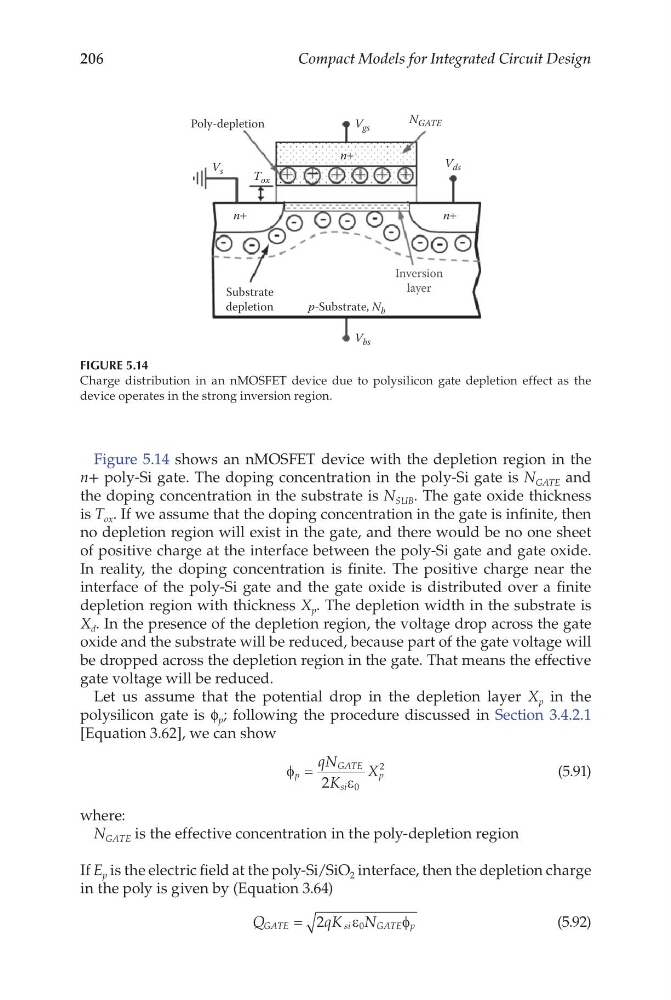
Figure 5.14 shows an nMOSFET device with the depletion region in the
n+ poly-Si gate. The doping concentration in the poly-Si gate is N GATE and
the doping concentration in the substrate is N SUB . The gate oxide thickness
is T ox . If we assume that the doping concentration in the gate is infinite, then
no depletion region will exist in the gate, and there would be no one sheet
of positive charge at the interface between the poly-Si gate and gate oxide.
In reality, the doping concentration is finite. The positive charge near the
interface of the poly-Si gate and the gate oxide is distributed over a finite
depletion region with thickness X p . The depletion width in the substrate is
X d . In the presence of the depletion region, the voltage drop across the gate
oxide and the substrate will be reduced, because part of the gate voltage will
be dropped across the depletion region in the gate. That means the effective
gate voltage will be reduced.
Let us assume that the potential drop in the depletion layer X p in the
polysilicon gate is f p ; following the procedure discussed in Section 3.4.2.1
[Equation 3.62], we can show
φ
ε
p
GATE
si
p
qN
K
X
= 2
0
2
(5.91)
where:
N GATE is the effective concentration in the poly-depletion region
If E p is the electric field at the poly-Si/SiO 2 interface, then the depletion charge
in the poly is given by (Equation 3.64)
Q
q K N
GATE
s i
GATE p
= 2
0
ε
φ
(5.92)
Poly-depletion
V s
V bs
Substrate
depletion
n+
n+
n+
Inversion
layer
p-Substrate, N b
T ox
N GATE
V gs
V ds
FIGURE 5.14
Charge distribution in an nMOSFET device due to polysilicon gate depletion effect as the
device operates in the strong inversion region.
Compact Models for Integrated Circuit Design
Figure 5.14 shows an nMOSFET device with the depletion region in the
n+ poly-Si gate. The doping concentration in the poly-Si gate is N GATE and
the doping concentration in the substrate is N SUB . The gate oxide thickness
is T ox . If we assume that the doping concentration in the gate is infinite, then
no depletion region will exist in the gate, and there would be no one sheet
of positive charge at the interface between the poly-Si gate and gate oxide.
In reality, the doping concentration is finite. The positive charge near the
interface of the poly-Si gate and the gate oxide is distributed over a finite
depletion region with thickness X p . The depletion width in the substrate is
X d . In the presence of the depletion region, the voltage drop across the gate
oxide and the substrate will be reduced, because part of the gate voltage will
be dropped across the depletion region in the gate. That means the effective
gate voltage will be reduced.
Let us assume that the potential drop in the depletion layer X p in the
polysilicon gate is f p ; following the procedure discussed in Section 3.4.2.1
[Equation 3.62], we can show
φ
ε
p
GATE
si
p
qN
K
X
= 2
0
2
(5.91)
where:
N GATE is the effective concentration in the poly-depletion region
If E p is the electric field at the poly-Si/SiO 2 interface, then the depletion charge
in the poly is given by (Equation 3.64)
Q
q K N
GATE
s i
GATE p
= 2
0
ε
φ
(5.92)
Poly-depletion
V s
V bs
Substrate
depletion
n+
n+
n+
Inversion
layer
p-Substrate, N b
T ox
N GATE
V gs
V ds
FIGURE 5.14
Charge distribution in an nMOSFET device due to polysilicon gate depletion effect as the
device operates in the strong inversion region.