

190
Compact Models for Integrated Circuit Design
∆L L
L
L
L
L
L
L L
INT
L
L
W
L
WL
L
L
LN
WN
LN
WN
=
+
+
+
(5.41)
∆W W
V
V
W
L
W
W
W
L
INT
g steff
s
bseff
s
L
W
W
W
WL
W
LN
WN
L
=
+
+
−
−
(
)
+
+
+
DWG
D WB
.
φ
φ
N N
W N
W
W
(5.42)
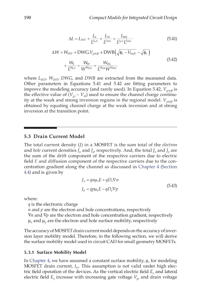
where L INT , W INT , DWG, and DWB are extracted from the measured data.
Other parameters in Equations 5.41 and 5.42 are fitting parameters to
improve the modeling accuracy (and rarely used). In Equation 5.42, V gsteff is
the effective value of (V gs − V th ) used to ensure the channel charge continuity at the weak and strong inversion regions in the regional model. V gsteff is
obtained by equating channel charge at the weak inversion and at strong
inversion at the transition point.
5.3 Drain Current Model
The total current density (J) in a MOSFET is the sum total of the electron
and hole current densities J n and J p , respectively. And, the total J n and J p are
the sum of the drift component of the respective carriers due to electric
field E and diffusion component of the respective carriers due to the concentration gradient along the channel as discussed in Chapter 4 (Section
4.4) and is given by
J qn E qD n
J qp E qD p
n
n
n
p
p
p
=
+
∇
=
−
∇
µ
µ
(5.43)
where:
q is the electronic charge
n and p are the electron and hole concentrations, respectively
∇n and ∇p are the electron and hole concentration gradient, respectively
μ n and μ p are the electron and hole surface mobility, respectively
The accuracy of MOSFET drain current model depends on the accuracy of inversion layer mobility model. Therefore, in the following section, we will derive
the surface mobility model used in circuit CAD for small geometry MOSFETs.
5.3.1 Surface Mobility Model
In Chapter 4, we have assumed a constant surface mobility, μ s for modeling
MOSFET drain current, I ds . This assumption is not valid under high electric field operation of the devices. As the vertical electric field E x and lateral
electric field E y increase with increasing gate voltage V gs and drain voltage
Compact Models for Integrated Circuit Design
∆L L
L
L
L
L
L
L L
INT
L
L
W
L
WL
L
L
LN
WN
LN
WN
=
+
+
+
(5.41)
∆W W
V
V
W
L
W
W
W
L
INT
g steff
s
bseff
s
L
W
W
W
WL
W
LN
WN
L
=
+
+
−
−
(
)
+
+
+
DWG
D WB
.
φ
φ
N N
W N
W
W
(5.42)
where L INT , W INT , DWG, and DWB are extracted from the measured data.
Other parameters in Equations 5.41 and 5.42 are fitting parameters to
improve the modeling accuracy (and rarely used). In Equation 5.42, V gsteff is
the effective value of (V gs − V th ) used to ensure the channel charge continuity at the weak and strong inversion regions in the regional model. V gsteff is
obtained by equating channel charge at the weak inversion and at strong
inversion at the transition point.
5.3 Drain Current Model
The total current density (J) in a MOSFET is the sum total of the electron
and hole current densities J n and J p , respectively. And, the total J n and J p are
the sum of the drift component of the respective carriers due to electric
field E and diffusion component of the respective carriers due to the concentration gradient along the channel as discussed in Chapter 4 (Section
4.4) and is given by
J qn E qD n
J qp E qD p
n
n
n
p
p
p
=
+
∇
=
−
∇
µ
µ
(5.43)
where:
q is the electronic charge
n and p are the electron and hole concentrations, respectively
∇n and ∇p are the electron and hole concentration gradient, respectively
μ n and μ p are the electron and hole surface mobility, respectively
The accuracy of MOSFET drain current model depends on the accuracy of inversion layer mobility model. Therefore, in the following section, we will derive
the surface mobility model used in circuit CAD for small geometry MOSFETs.
5.3.1 Surface Mobility Model
In Chapter 4, we have assumed a constant surface mobility, μ s for modeling
MOSFET drain current, I ds . This assumption is not valid under high electric field operation of the devices. As the vertical electric field E x and lateral
electric field E y increase with increasing gate voltage V gs and drain voltage