

189
Compact Models for Small Geometry MOSFETs
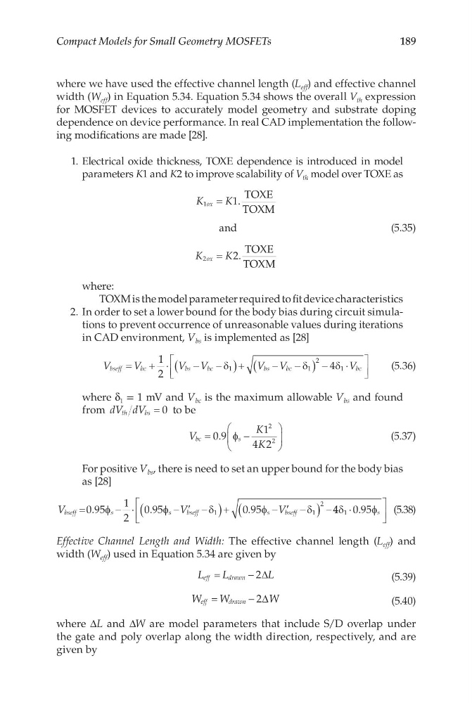
where we have used the effective channel length (L eff ) and effective channel
width (W eff ) in Equation 5.34. Equation 5.34 shows the overall V th expression
for MOSFET devices to accurately model geometry and substrate doping
dependence on device performance. In real CAD implementation the following modifications are made [28].
1. Electrical oxide thickness, TOXE dependence is introduced in model
parameters K1 and K2 to improve scalability of V th model over TOXE as
K
K
K
K
ox
ox
1
2
1
2
=
=
.
.
TOXE
TOXM
and
TOXE
TOXM
(5.35)
where:
TOXM is the model parameter required to fit device characteristics
2. In order to set a lower bound for the body bias during circuit simulations to prevent occurrence of unreasonable values during iterations
in CAD environment, V bs is implemented as [28]
V
V
V V
V V
V
bseff
b c
b s
b c
b s
b c
b c
=
+ ⋅
−
−
(
)+
−
−
(
)− ⋅
1
2
4
1
1
2
1
δ
δ
δ
(5.36)
where δ 1 = 1 mV and V bc is the maximum allowable V bs and found
from dV dV
th
bs = 0 to be
V
K
K
bc
s
=
−
0 9
1
4 2
2
2
. φ
(5.37)
For positive V bs , there is need to set an upper bound for the body bias
as [28]
V
V
V
bseff
s
s
b seff
s
bseff
=
− ⋅
− ′ −
(
) +
− ′ −
(
) −
0 95
1
2
0 95
0 95
1
1
2
.
.
.
φ
φ
δ
φ
δ
4 4 0 95
1
δ
φ
⋅
.
s
(5.38)
Effective Channel Length and Width: The effective channel length (L eff ) and
width (W eff ) used in Equation 5.34 are given by
L
L
L
eff
d rawn
=
−2∆
(5.39)
W
W
W
eff
d rawn
=
−2∆
(5.40)
where ΔL and ΔW are model parameters that include S/D overlap under
the gate and poly overlap along the width direction, respectively, and are
given by
Compact Models for Small Geometry MOSFETs
where we have used the effective channel length (L eff ) and effective channel
width (W eff ) in Equation 5.34. Equation 5.34 shows the overall V th expression
for MOSFET devices to accurately model geometry and substrate doping
dependence on device performance. In real CAD implementation the following modifications are made [28].
1. Electrical oxide thickness, TOXE dependence is introduced in model
parameters K1 and K2 to improve scalability of V th model over TOXE as
K
K
K
K
ox
ox
1
2
1
2
=
=
.
.
TOXE
TOXM
and
TOXE
TOXM
(5.35)
where:
TOXM is the model parameter required to fit device characteristics
2. In order to set a lower bound for the body bias during circuit simulations to prevent occurrence of unreasonable values during iterations
in CAD environment, V bs is implemented as [28]
V
V
V V
V V
V
bseff
b c
b s
b c
b s
b c
b c
=
+ ⋅
−
−
(
)+
−
−
(
)− ⋅
1
2
4
1
1
2
1
δ
δ
δ
(5.36)
where δ 1 = 1 mV and V bc is the maximum allowable V bs and found
from dV dV
th
bs = 0 to be
V
K
K
bc
s
=
−
0 9
1
4 2
2
2
. φ
(5.37)
For positive V bs , there is need to set an upper bound for the body bias
as [28]
V
V
V
bseff
s
s
b seff
s
bseff
=
− ⋅
− ′ −
(
) +
− ′ −
(
) −
0 95
1
2
0 95
0 95
1
1
2
.
.
.
φ
φ
δ
φ
δ
4 4 0 95
1
δ
φ
⋅
.
s
(5.38)
Effective Channel Length and Width: The effective channel length (L eff ) and
width (W eff ) used in Equation 5.34 are given by
L
L
L
eff
d rawn
=
−2∆
(5.39)
W
W
W
eff
d rawn
=
−2∆
(5.40)
where ΔL and ΔW are model parameters that include S/D overlap under
the gate and poly overlap along the width direction, respectively, and are
given by