

191
Compact Models for Small Geometry MOSFETs
V ds , respectively, the inversion carriers suffer increased scattering. Therefore,
μ s strongly depends on E x and E y . Let us consider the effect of E x only on
the surface mobility, that is, V ds ~ 0. For the simplicity of I ds modeling, let us
define an effective mobility as the average mobility of carriers given by
µ
µ
eff
s
X
X
x y n x y dx
n x y dx
inv
inv
=
⋅
∫
∫
( , ) ( , )
( , )
0
0
(5.44)
Using the definition of mobility from Equation 5.44 in Equation 4.64, we can
write
I
W
L
Q dV
ds
eff
i
Vds
=
∫
µ
0
(5.45)
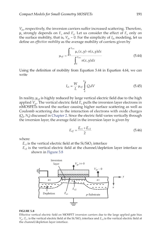
In reality, μ eff is highly reduced by large vertical electric field due to the high
applied V gs . The vertical electric field E x pulls the inversion layer electrons in
nMOSFETs toward the surface causing higher surface scattering as well as
Coulomb scattering due to the interaction of electrons with oxide charges
(Q f , N it ) discussed in Chapter 2. Since the electric field varies vertically through
the inversion layer, the average field in the inversion layer is given by
E
E
E
eff
x
x
=
+
1
2
2
(5.46)
where:
E x1 is the vertical electric field at the Si/SiO 2 interface
E x2 is the vertical electric field at the channel/depletion layer interface as
shown in Figure 5.8
Inversion
layer
Depletion
E x1
p-Substrate
x
y
E x2
n+
n+
V gs >> 0
V ds ∼ 0
FIGURE 5.8
Effective vertical electric field on MOSFET inversion carriers due to the large applied gate bias
V gs : E x1 is the vertical electric field at the Si/SiO 2 interface and E x2 is the vertical electric field at
the channel/depletion layer interface.
Compact Models for Small Geometry MOSFETs
V ds , respectively, the inversion carriers suffer increased scattering. Therefore,
μ s strongly depends on E x and E y . Let us consider the effect of E x only on
the surface mobility, that is, V ds ~ 0. For the simplicity of I ds modeling, let us
define an effective mobility as the average mobility of carriers given by
µ
µ
eff
s
X
X
x y n x y dx
n x y dx
inv
inv
=
⋅
∫
∫
( , ) ( , )
( , )
0
0
(5.44)
Using the definition of mobility from Equation 5.44 in Equation 4.64, we can
write
I
W
L
Q dV
ds
eff
i
Vds
=
∫
µ
0
(5.45)
In reality, μ eff is highly reduced by large vertical electric field due to the high
applied V gs . The vertical electric field E x pulls the inversion layer electrons in
nMOSFETs toward the surface causing higher surface scattering as well as
Coulomb scattering due to the interaction of electrons with oxide charges
(Q f , N it ) discussed in Chapter 2. Since the electric field varies vertically through
the inversion layer, the average field in the inversion layer is given by
E
E
E
eff
x
x
=
+
1
2
2
(5.46)
where:
E x1 is the vertical electric field at the Si/SiO 2 interface
E x2 is the vertical electric field at the channel/depletion layer interface as
shown in Figure 5.8
Inversion
layer
Depletion
E x1
p-Substrate
x
y
E x2
n+
n+
V gs >> 0
V ds ∼ 0
FIGURE 5.8
Effective vertical electric field on MOSFET inversion carriers due to the large applied gate bias
V gs : E x1 is the vertical electric field at the Si/SiO 2 interface and E x2 is the vertical electric field at
the channel/depletion layer interface.