

186
Compact Models for Integrated Circuit Design
∆V
V V
th
th
bs
ds
(
)
(
)
DIBL
DIBL ETA ETAB
= −
⋅
+
⋅
(
) ⋅
θ
0
(5.28)
where l t0 is the characteristics length without bias and is given by
l
K T W
K
t
si ox d
ox
0
0
=
η
(5.29)
with zero bias depletion width is given by (Equation 2.97), W
K
qN
d
s i
s
CH
0
0
2
=
εφ
.
In summary, the parameters used in BSIM4 (Berkeley Short Channel
IGFET Model, version 4) compact MOS models for SCE and DIBL modeling
are DVT0, DVT1, DVT2, DSUB, ETA0, and ETAB. Where, DVT2 and ETAB
account for substrate bias effect on SCE and DIBL, respectively.
5.2.2.2 Threshold Voltage Modeling for Narrow
Channel MOSFET Devices
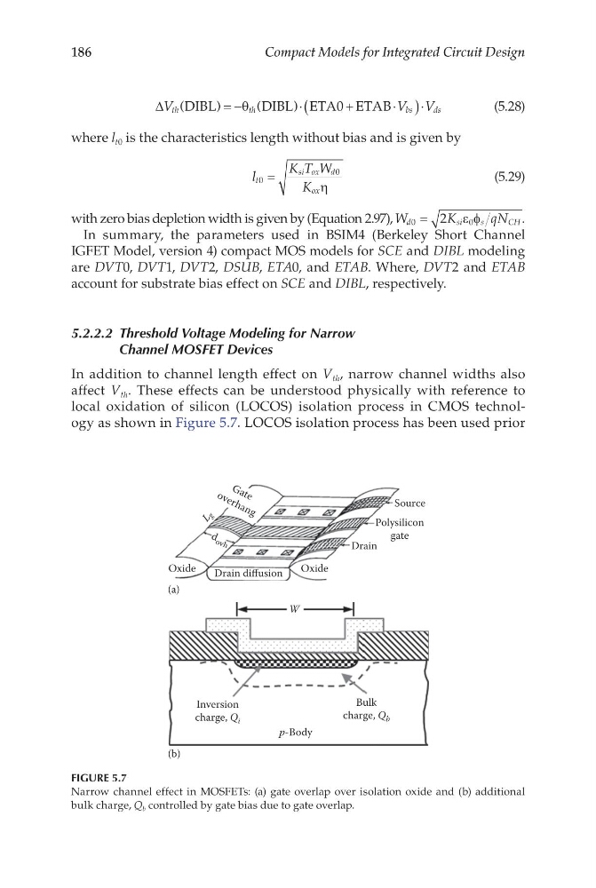
In addition to channel length effect on V th , narrow channel widths also
affect V th . These effects can be understood physically with reference to
local oxidation of silicon (LOCOS) isolation process in CMOS technology as shown in Figure 5.7. LOCOS isolation process has been used prior
Oxide
(a)
L g
Oxide
Drain
Polysilicon
gate
Source
G a t e
o v e r h a n g
d o v h
Drain diffusion
p-Body
Inversion
charge, Q i
W
Bulk
charge, Q b
(b)
FIGURE 5.7
Narrow channel effect in MOSFETs: (a) gate overlap over isolation oxide and (b) additional
bulk charge, Q b controlled by gate bias due to gate overlap.
Compact Models for Integrated Circuit Design
∆V
V V
th
th
bs
ds
(
)
(
)
DIBL
DIBL ETA ETAB
= −
⋅
+
⋅
(
) ⋅
θ
0
(5.28)
where l t0 is the characteristics length without bias and is given by
l
K T W
K
t
si ox d
ox
0
0
=
η
(5.29)
with zero bias depletion width is given by (Equation 2.97), W
K
qN
d
s i
s
CH
0
0
2
=
εφ
.
In summary, the parameters used in BSIM4 (Berkeley Short Channel
IGFET Model, version 4) compact MOS models for SCE and DIBL modeling
are DVT0, DVT1, DVT2, DSUB, ETA0, and ETAB. Where, DVT2 and ETAB
account for substrate bias effect on SCE and DIBL, respectively.
5.2.2.2 Threshold Voltage Modeling for Narrow
Channel MOSFET Devices
In addition to channel length effect on V th , narrow channel widths also
affect V th . These effects can be understood physically with reference to
local oxidation of silicon (LOCOS) isolation process in CMOS technology as shown in Figure 5.7. LOCOS isolation process has been used prior
Oxide
(a)
L g
Oxide
Drain
Polysilicon
gate
Source
G a t e
o v e r h a n g
d o v h
Drain diffusion
p-Body
Inversion
charge, Q i
W
Bulk
charge, Q b
(b)
FIGURE 5.7
Narrow channel effect in MOSFETs: (a) gate overlap over isolation oxide and (b) additional
bulk charge, Q b controlled by gate bias due to gate overlap.