

187
Compact Models for Small Geometry MOSFETs
to shallow trench isolation (STI) techniques used in advanced CMOS
technology.
Figure 5.7b shows two-dimensional (2D) cross-section of a MOSFET
device along the channel width direction from the layout shown in
Figure 5.7a. As shown in Figure 5.7b, the depletion layer does not abruptly
change from deep to shallow at the edge of gate oxide. Therefore, there is
a transition region and some spreading of field lines outside W. Thus, the
gate charge Q g supports some charge outside W. Since Q g = Q b + Q i , for
the same gate bias, Q b is higher for narrow devices (i.e., gate is required to
induce more Q b out of the same Q g ), resulting in lower Q i and consequently
higher V th .
For STI devices, the fringing field from the gate regions beyond the channel
edges support channel depletion charges. This fringing field causes deeper
depletion resulting in higher band bending and, therefore, an increase in the
surface potential f s near the STI channel edge. The higher f s induces channel inversion near the STI at a lower V gs than the rest of the channel. Thus, it
takes lower effective V gs to reach maximum channel depletion and the formation of inversion layer. Since the percentage contribution of the fringing
field increases as the channel width W decreases, V th tends to decrease with
decreasing W in MOSFETs using STI technology (in contrast to LOCOS isolation technology), resulting in inverse NWE.
The physics of NWE can be understood by charge-sharing model similar
to SCE [32]. However, these models are not suitable for compact modeling of
billions of transistors in a VLSI circuit. Besides, NWE depends on the isolation technology. Therefore, universally accurate physical model is not available. For compact modeling, an empirical model can be developed, based
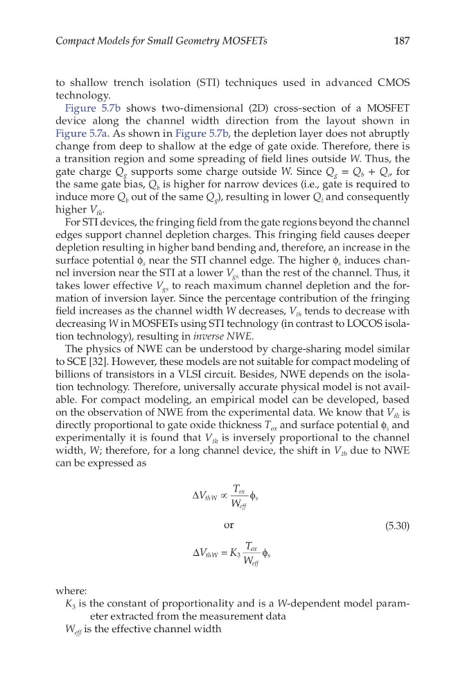
on the observation of NWE from the experimental data. We know that V th is
directly proportional to gate oxide thickness T ox and surface potential f s and
experimentally it is found that V th is inversely proportional to the channel
width, W; therefore, for a long channel device, the shift in V th due to NWE
can be expressed as
∆
∆
V
T
W
V
K
T
W
thW
ox
eff
s
thW
ox
eff
s
∝
=
φ
φ
or
3
(5.30)
where:
K 3 is the constant of proportionality and is a W-dependent model parameter extracted from the measurement data
W eff is the effective channel width
Compact Models for Small Geometry MOSFETs
to shallow trench isolation (STI) techniques used in advanced CMOS
technology.
Figure 5.7b shows two-dimensional (2D) cross-section of a MOSFET
device along the channel width direction from the layout shown in
Figure 5.7a. As shown in Figure 5.7b, the depletion layer does not abruptly
change from deep to shallow at the edge of gate oxide. Therefore, there is
a transition region and some spreading of field lines outside W. Thus, the
gate charge Q g supports some charge outside W. Since Q g = Q b + Q i , for
the same gate bias, Q b is higher for narrow devices (i.e., gate is required to
induce more Q b out of the same Q g ), resulting in lower Q i and consequently
higher V th .
For STI devices, the fringing field from the gate regions beyond the channel
edges support channel depletion charges. This fringing field causes deeper
depletion resulting in higher band bending and, therefore, an increase in the
surface potential f s near the STI channel edge. The higher f s induces channel inversion near the STI at a lower V gs than the rest of the channel. Thus, it
takes lower effective V gs to reach maximum channel depletion and the formation of inversion layer. Since the percentage contribution of the fringing
field increases as the channel width W decreases, V th tends to decrease with
decreasing W in MOSFETs using STI technology (in contrast to LOCOS isolation technology), resulting in inverse NWE.
The physics of NWE can be understood by charge-sharing model similar
to SCE [32]. However, these models are not suitable for compact modeling of
billions of transistors in a VLSI circuit. Besides, NWE depends on the isolation technology. Therefore, universally accurate physical model is not available. For compact modeling, an empirical model can be developed, based
on the observation of NWE from the experimental data. We know that V th is
directly proportional to gate oxide thickness T ox and surface potential f s and
experimentally it is found that V th is inversely proportional to the channel
width, W; therefore, for a long channel device, the shift in V th due to NWE
can be expressed as
∆
∆
V
T
W
V
K
T
W
thW
ox
eff
s
thW
ox
eff
s
∝
=
φ
φ
or
3
(5.30)
where:
K 3 is the constant of proportionality and is a W-dependent model parameter extracted from the measurement data
W eff is the effective channel width