

185
Compact Models for Small Geometry MOSFETs
where N CH and N SD are the effective channel and S/D doping concentrations,
respectively, and l t represents the characteristic length given by
l
K T W
K
t
si ox d
ox
=
η
(5.23)
With depletion width W
K
V qN
d
s i
s
bs
CH
=
−
(
)
2
0
ε φ
and η (ETA) is a fitting
parameter so that W d /η = average width of the depletion region along the
length of the channel.
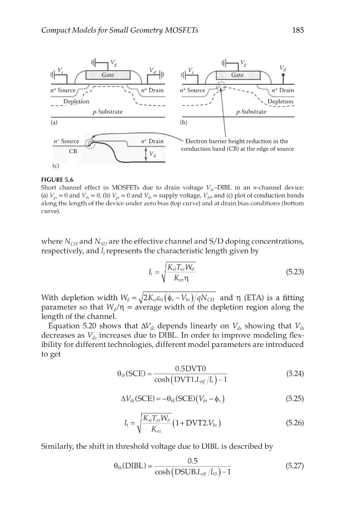
Equation 5.20 shows that ΔV th depends linearly on V ds showing that V th
decreases as V ds increases due to DIBL. In order to improve modeling flexibility for different technologies, different model parameters are introduced
to get
θ th
eff t
L l
(
)
.
cosh
.
SCE
DVT
DVT
=
(
) −
0 5
0
1
1
(5.24)
∆V
V
th
th
bi
s
(
)
(
)
SCE
S CE
= −
−
(
)
θ
φ
(5.25)
l
K T W
K
V
t
si ox d
ox
bs
=
+
(
)
1
2
DVT .
(5.26)
Similarly, the shift in threshold voltage due to DIBL is described by
θ th
eff t
L l
(
)
.
cosh
.
DIBL
DSUB
=
(
) −
0 5
1
0
(5.27)
V s
V g
V g
Gate
Electron barrier height reduction in the
conduction band (CB) at the edge of source
Gate
Depletion
CB
p-Substrate
n + Source
n + Source
n + Drain
n + Drain
Depletion
p-Substrate
n + Source
n + Drain
V d
V d
V d
V s
(a)
(b)
(c)
FIGURE 5.6
Short channel effect in MOSFETs due to drain voltage V ds –DIBL in an n-channel device:
(a) V gs = 0 and V ds = 0, (b) V gs = 0 and V ds = supply voltage, V dd , and (c) plot of conduction bands
along the length of the device under zero bias (top curve) and at drain bias conditions (bottom
curve).
Compact Models for Small Geometry MOSFETs
where N CH and N SD are the effective channel and S/D doping concentrations,
respectively, and l t represents the characteristic length given by
l
K T W
K
t
si ox d
ox
=
η
(5.23)
With depletion width W
K
V qN
d
s i
s
bs
CH
=
−
(
)
2
0
ε φ
and η (ETA) is a fitting
parameter so that W d /η = average width of the depletion region along the
length of the channel.
Equation 5.20 shows that ΔV th depends linearly on V ds showing that V th
decreases as V ds increases due to DIBL. In order to improve modeling flexibility for different technologies, different model parameters are introduced
to get
θ th
eff t
L l
(
)
.
cosh
.
SCE
DVT
DVT
=
(
) −
0 5
0
1
1
(5.24)
∆V
V
th
th
bi
s
(
)
(
)
SCE
S CE
= −
−
(
)
θ
φ
(5.25)
l
K T W
K
V
t
si ox d
ox
bs
=
+
(
)
1
2
DVT .
(5.26)
Similarly, the shift in threshold voltage due to DIBL is described by
θ th
eff t
L l
(
)
.
cosh
.
DIBL
DSUB
=
(
) −
0 5
1
0
(5.27)
V s
V g
V g
Gate
Electron barrier height reduction in the
conduction band (CB) at the edge of source
Gate
Depletion
CB
p-Substrate
n + Source
n + Source
n + Drain
n + Drain
Depletion
p-Substrate
n + Source
n + Drain
V d
V d
V d
V s
(a)
(b)
(c)
FIGURE 5.6
Short channel effect in MOSFETs due to drain voltage V ds –DIBL in an n-channel device:
(a) V gs = 0 and V ds = 0, (b) V gs = 0 and V ds = supply voltage, V dd , and (c) plot of conduction bands
along the length of the device under zero bias (top curve) and at drain bias conditions (bottom
curve).