

183
Compact Models for Small Geometry MOSFETs
• K 1 and K 2 model the effect of nonuniform vertical channel doping
profile on V th ;
• L PE0 and L PEB model the nonuniform lateral channel doping profile
on V th at V bs = 0 and |V bs | > 0, respectively;
• At V bs = 0, as L decreases, Equation 5.18 shows that V th increases,
showing reverse short channel effect due to halo-doping profile as
shown in Figure 5.2b.
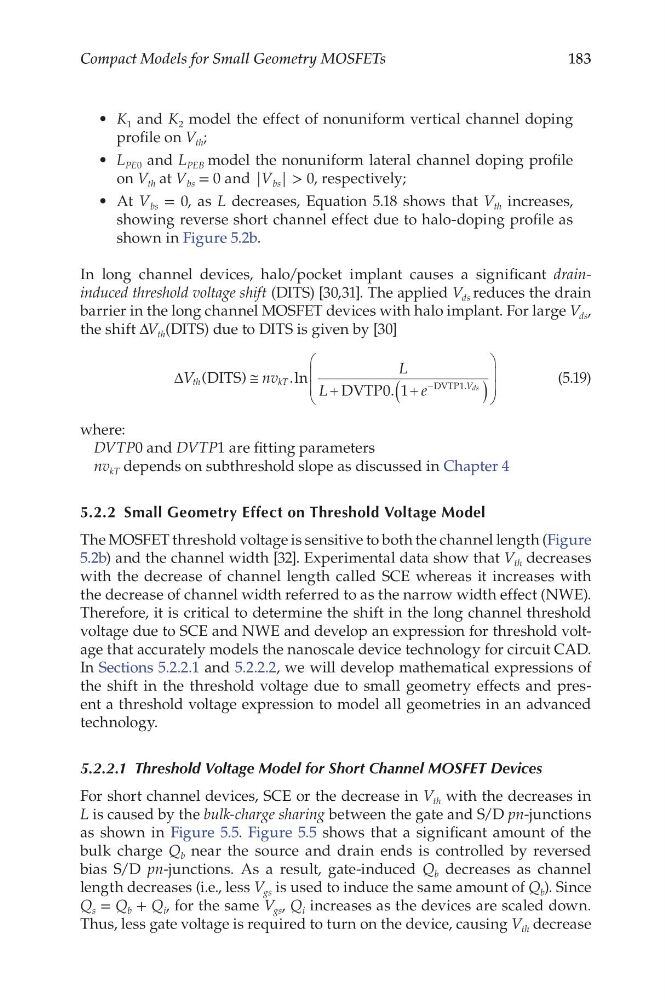
In long channel devices, halo/pocket implant causes a significant draininduced threshold voltage shift (DITS) [30,31]. The applied V ds reduces the drain
barrier in the long channel MOSFET devices with halo implant. For large V ds ,
the shift ΔV th (DITS) due to DITS is given by [30]
∆V
n v
L
L
e
th
kT
Vds
(
)
.ln
.
.
DITS
DVTP
DVTP
≅
+
+
(
)
−
0 1
1
(5.19)
where:
DVTP0 and DVTP1 are fitting parameters
nv kT depends on subthreshold slope as discussed in Chapter 4
5.2.2 Small Geometry Effect on Threshold Voltage Model
The MOSFET threshold voltage is sensitive to both the channel length (Figure
5.2b) and the channel width [32]. Experimental data show that V th decreases
with the decrease of channel length called SCE whereas it increases with
the decrease of channel width referred to as the narrow width effect (NWE).
Therefore, it is critical to determine the shift in the long channel threshold
voltage due to SCE and NWE and develop an expression for threshold voltage that accurately models the nanoscale device technology for circuit CAD.
In Sections 5.2.2.1 and 5.2.2.2, we will develop mathematical expressions of
the shift in the threshold voltage due to small geometry effects and present a threshold voltage expression to model all geometries in an advanced
technology.
5.2.2.1 Threshold Voltage Model for Short Channel MOSFET Devices
For short channel devices, SCE or the decrease in V th with the decreases in
L is caused by the bulk-charge sharing between the gate and S/D pn-junctions
as shown in Figure 5.5. Figure 5.5 shows that a significant amount of the
bulk charge Q b near the source and drain ends is controlled by reversed
bias S/D pn-junctions. As a result, gate-induced Q b decreases as channel
length decreases (i.e., less V gs is used to induce the same amount of Q b ). Since
Q s = Q b + Q i , for the same V gs , Q i increases as the devices are scaled down.
Thus, less gate voltage is required to turn on the device, causing V th decrease
Compact Models for Small Geometry MOSFETs
• K 1 and K 2 model the effect of nonuniform vertical channel doping
profile on V th ;
• L PE0 and L PEB model the nonuniform lateral channel doping profile
on V th at V bs = 0 and |V bs | > 0, respectively;
• At V bs = 0, as L decreases, Equation 5.18 shows that V th increases,
showing reverse short channel effect due to halo-doping profile as
shown in Figure 5.2b.
In long channel devices, halo/pocket implant causes a significant draininduced threshold voltage shift (DITS) [30,31]. The applied V ds reduces the drain
barrier in the long channel MOSFET devices with halo implant. For large V ds ,
the shift ΔV th (DITS) due to DITS is given by [30]
∆V
n v
L
L
e
th
kT
Vds
(
)
.ln
.
.
DITS
DVTP
DVTP
≅
+
+
(
)
−
0 1
1
(5.19)
where:
DVTP0 and DVTP1 are fitting parameters
nv kT depends on subthreshold slope as discussed in Chapter 4
5.2.2 Small Geometry Effect on Threshold Voltage Model
The MOSFET threshold voltage is sensitive to both the channel length (Figure
5.2b) and the channel width [32]. Experimental data show that V th decreases
with the decrease of channel length called SCE whereas it increases with
the decrease of channel width referred to as the narrow width effect (NWE).
Therefore, it is critical to determine the shift in the long channel threshold
voltage due to SCE and NWE and develop an expression for threshold voltage that accurately models the nanoscale device technology for circuit CAD.
In Sections 5.2.2.1 and 5.2.2.2, we will develop mathematical expressions of
the shift in the threshold voltage due to small geometry effects and present a threshold voltage expression to model all geometries in an advanced
technology.
5.2.2.1 Threshold Voltage Model for Short Channel MOSFET Devices
For short channel devices, SCE or the decrease in V th with the decreases in
L is caused by the bulk-charge sharing between the gate and S/D pn-junctions
as shown in Figure 5.5. Figure 5.5 shows that a significant amount of the
bulk charge Q b near the source and drain ends is controlled by reversed
bias S/D pn-junctions. As a result, gate-induced Q b decreases as channel
length decreases (i.e., less V gs is used to induce the same amount of Q b ). Since
Q s = Q b + Q i , for the same V gs , Q i increases as the devices are scaled down.
Thus, less gate voltage is required to turn on the device, causing V th decrease