

182
Compact Models for Integrated Circuit Design
where:
L PEB is a model parameter obtained by optimizing I–V data for different V bs
for short channel and wide MOSFET devices
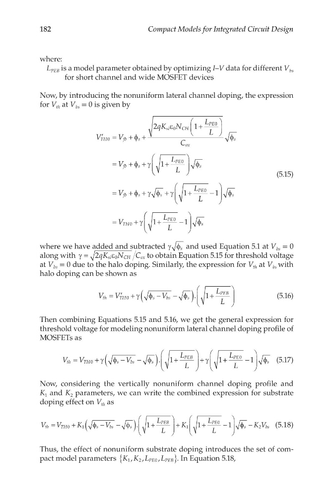
Now, by introducing the nonuniform lateral channel doping, the expression
for V th at V bs = 0 is given by
′ =
+ +
+
=
+ +
+
V
V
qK N
L
L
C
V
L
L
TH
fb
s
si
CH
PE
ox
s
fb
s
PE
0
0
0
0
2
1
1
φ
ε
φ
φ γ
=
+ +
+
+
−
=
+
+
−
φ
φ γ φ γ
φ
γ
s
fb
s
s
PE
s
TH
PE
V
L
L
V
L
L
1
1
1
1
0
0
0
φ s
(5.15)
where we have added and subtracted γ φ s and used Equation 5.1 at V bs = 0
along with γ
ε
= 2
0
qK N
C
si
CH
ox to obtain Equation 5.15 for threshold voltage
at V bs = 0 due to the halo doping. Similarly, the expression for V th at V bs with
halo doping can be shown as
V V
V
L
L
th
TH
s
b s
s
PEB
= ′ +
−
−
(
) +
0
1
γ φ
φ .
(5.16)
Then combining Equations 5.15 and 5.16, we get the general expression for
threshold voltage for modeling nonuniform lateral channel doping profile of
MOSFETs as
V V
V
L
L
L
L
th
TH
s
b s
s
PEB
PE
s
=
+
−
−
(
) +
+
+
−
0
0
1
1
1
γ φ
φ
γ
φ
.
(5.17)
Now, considering the vertically nonuniform channel doping profile and
K 1 and K 2 parameters, we can write the combined expression for substrate
doping effect on V th as
V V
K
V
L
L
K
L
L
th
TH
s
b s
s
PEB
PE
=
+
−
−
(
) +
+
+
−
0
1
1
0
1
1
1
φ
φ .
φ φ s
b s
K V
− 2
(5.18)
Thus, the effect of nonuniform substrate doping introduces the set of compact model parameters K K L
L
PE
PEB
1
2
0
, ,
,
{
} . In Equation 5.18,
Compact Models for Integrated Circuit Design
where:
L PEB is a model parameter obtained by optimizing I–V data for different V bs
for short channel and wide MOSFET devices
Now, by introducing the nonuniform lateral channel doping, the expression
for V th at V bs = 0 is given by
′ =
+ +
+
=
+ +
+
V
V
qK N
L
L
C
V
L
L
TH
fb
s
si
CH
PE
ox
s
fb
s
PE
0
0
0
0
2
1
1
φ
ε
φ
φ γ
=
+ +
+
+
−
=
+
+
−
φ
φ γ φ γ
φ
γ
s
fb
s
s
PE
s
TH
PE
V
L
L
V
L
L
1
1
1
1
0
0
0
φ s
(5.15)
where we have added and subtracted γ φ s and used Equation 5.1 at V bs = 0
along with γ
ε
= 2
0
qK N
C
si
CH
ox to obtain Equation 5.15 for threshold voltage
at V bs = 0 due to the halo doping. Similarly, the expression for V th at V bs with
halo doping can be shown as
V V
V
L
L
th
TH
s
b s
s
PEB
= ′ +
−
−
(
) +
0
1
γ φ
φ .
(5.16)
Then combining Equations 5.15 and 5.16, we get the general expression for
threshold voltage for modeling nonuniform lateral channel doping profile of
MOSFETs as
V V
V
L
L
L
L
th
TH
s
b s
s
PEB
PE
s
=
+
−
−
(
) +
+
+
−
0
0
1
1
1
γ φ
φ
γ
φ
.
(5.17)
Now, considering the vertically nonuniform channel doping profile and
K 1 and K 2 parameters, we can write the combined expression for substrate
doping effect on V th as
V V
K
V
L
L
K
L
L
th
TH
s
b s
s
PEB
PE
=
+
−
−
(
) +
+
+
−
0
1
1
0
1
1
1
φ
φ .
φ φ s
b s
K V
− 2
(5.18)
Thus, the effect of nonuniform substrate doping introduces the set of compact model parameters K K L
L
PE
PEB
1
2
0
, ,
,
{
} . In Equation 5.18,