

169
Large Geometry MOSFET Compact Models
d
I
dV
nv
dV
d
I
nv
ds
gs
kT
gs
ds
kT
ln
ln
(
)=
(
)
=
or
(4.126)
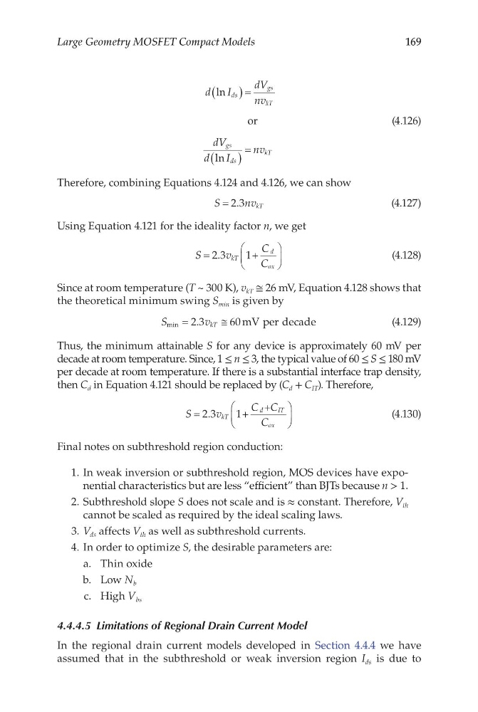
Therefore, combining Equations 4.124 and 4.126, we can show
S
nv kT
= 2 3
.
(4.127)
Using Equation 4.121 for the ideality factor n, we get
S
v
C
C
kT
d
ox
=
+
2 3
1
.
(4.128)
Since at room temperature (T ~ 300 K), v kT ≅ 26 mV, Equation 4.128 shows that
the theoretical minimum swing S min is given by
S
v kT
min
.
=
≅
2 3
60 mV per decade
(4.129)
Thus, the minimum attainable S for any device is approximately 60 mV per
decade at room temperature. Since, 1 ≤ n ≤ 3, the typical value of 60 ≤ S ≤ 180 mV
per decade at room temperature. If there is a substantial interface trap density,
then C d in Equation 4.121 should be replaced by (C d + C IT ). Therefore,
S
v
C C
C
kT
d
I T
ox
=
+
+
2 3
1
.
(4.130)
Final notes on subthreshold region conduction:
1. In weak inversion or subthreshold region, MOS devices have exponential characteristics but are less “efficient” than BJTs because n > 1.
2. Subthreshold slope S does not scale and is ≈ constant. Therefore, V th
cannot be scaled as required by the ideal scaling laws.
3. V ds affects V th as well as subthreshold currents.
4. In order to optimize S, the desirable parameters are:
a. Thin oxide
b. Low N b
c. High V bs
4.4.4.5 Limitations of Regional Drain Current Model
In the regional drain current models developed in Section 4.4.4 we have
assumed that in the subthreshold or weak inversion region I ds is due to
Large Geometry MOSFET Compact Models
d
I
dV
nv
dV
d
I
nv
ds
gs
kT
gs
ds
kT
ln
ln
(
)=
(
)
=
or
(4.126)
Therefore, combining Equations 4.124 and 4.126, we can show
S
nv kT
= 2 3
.
(4.127)
Using Equation 4.121 for the ideality factor n, we get
S
v
C
C
kT
d
ox
=
+
2 3
1
.
(4.128)
Since at room temperature (T ~ 300 K), v kT ≅ 26 mV, Equation 4.128 shows that
the theoretical minimum swing S min is given by
S
v kT
min
.
=
≅
2 3
60 mV per decade
(4.129)
Thus, the minimum attainable S for any device is approximately 60 mV per
decade at room temperature. Since, 1 ≤ n ≤ 3, the typical value of 60 ≤ S ≤ 180 mV
per decade at room temperature. If there is a substantial interface trap density,
then C d in Equation 4.121 should be replaced by (C d + C IT ). Therefore,
S
v
C C
C
kT
d
I T
ox
=
+
+
2 3
1
.
(4.130)
Final notes on subthreshold region conduction:
1. In weak inversion or subthreshold region, MOS devices have exponential characteristics but are less “efficient” than BJTs because n > 1.
2. Subthreshold slope S does not scale and is ≈ constant. Therefore, V th
cannot be scaled as required by the ideal scaling laws.
3. V ds affects V th as well as subthreshold currents.
4. In order to optimize S, the desirable parameters are:
a. Thin oxide
b. Low N b
c. High V bs
4.4.4.5 Limitations of Regional Drain Current Model
In the regional drain current models developed in Section 4.4.4 we have
assumed that in the subthreshold or weak inversion region I ds is due to