

154
Compact Models for Integrated Circuit Design
Equation 4.72 shows that I ds varies linearly with V ds . Consequently, this
region of MOSFET device performance is called the linear region operation.
From Equation 4.75, we get
V
I
V V
V
R
ds
ds
gs
th
gst
ch
≅
−
=
≡
1
1
β
β
(4.76)
where:
R ch is called the channel resistance and is the effective resistance between
the source and drain regions of MOSFET channel
Note that R ch varies linearly with (V gs − V th ) ≡ V gst . V gst is referred to as the effective gate voltage or gate over drive voltage. Thus, MOSFET devices are sometime
referred to as the voltage-controlled variable resistors.
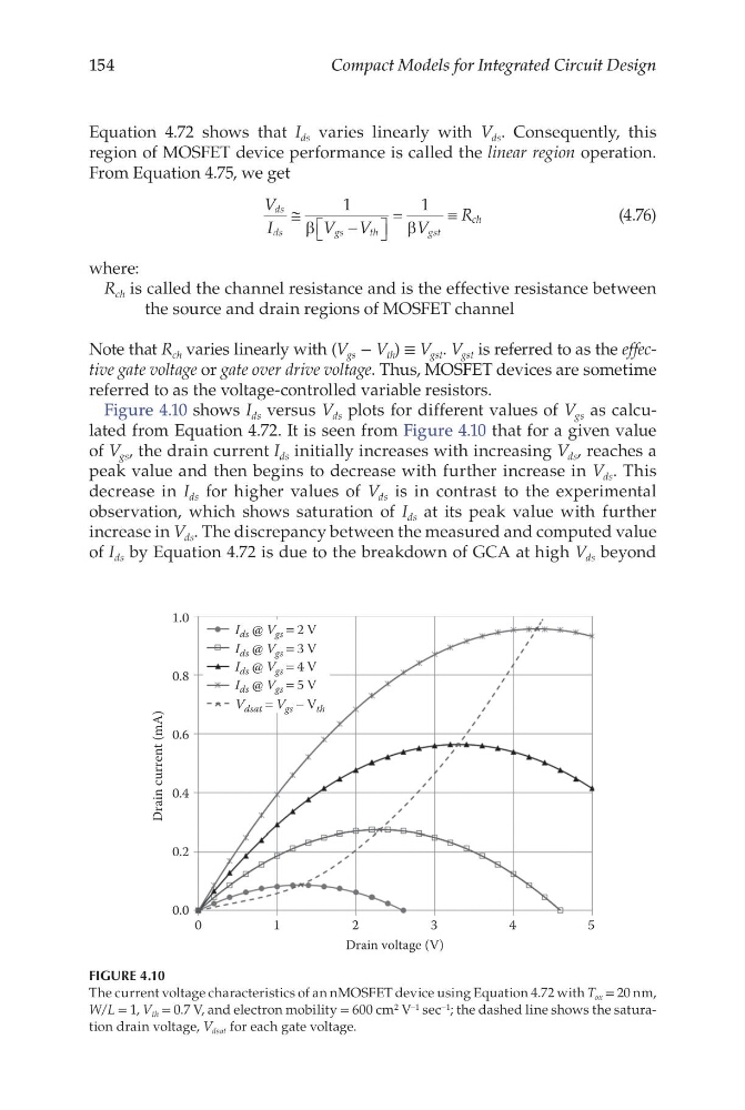
Figure 4.10 shows I ds versus V ds plots for different values of V gs as calculated from Equation 4.72. It is seen from Figure 4.10 that for a given value
of V gs , the drain current I ds initially increases with increasing V ds , reaches a
peak value and then begins to decrease with further increase in V ds . This
decrease in I ds for higher values of V ds is in contrast to the experimental
observation, which shows saturation of I ds at its peak value with further
increase in V ds . The discrepancy between the measured and computed value
of I ds by Equation 4.72 is due to the breakdown of GCA at high V ds beyond
0
0.0
0.2
0.4
Drain current (mA)
0.6
0.8
1.0
I ds @ V gs = 2 V
I ds @ V gs = 3 V
I ds @ V gs = 4 V
I ds @ V gs = 5 V
V dsat = V gs − V th
1
2
Drain voltage (V)
3
4
5
FIGURE 4.10
The current voltage characteristics of an nMOSFET device using Equation 4.72 with T ox = 20 nm,
W/L = 1, V th = 0.7 V, and electron mobility = 600 cm 2 V −1 sec −1 ; the dashed line shows the saturation drain voltage, V dsat for each gate voltage.
Compact Models for Integrated Circuit Design
Equation 4.72 shows that I ds varies linearly with V ds . Consequently, this
region of MOSFET device performance is called the linear region operation.
From Equation 4.75, we get
V
I
V V
V
R
ds
ds
gs
th
gst
ch
≅
−
=
≡
1
1
β
β
(4.76)
where:
R ch is called the channel resistance and is the effective resistance between
the source and drain regions of MOSFET channel
Note that R ch varies linearly with (V gs − V th ) ≡ V gst . V gst is referred to as the effective gate voltage or gate over drive voltage. Thus, MOSFET devices are sometime
referred to as the voltage-controlled variable resistors.
Figure 4.10 shows I ds versus V ds plots for different values of V gs as calculated from Equation 4.72. It is seen from Figure 4.10 that for a given value
of V gs , the drain current I ds initially increases with increasing V ds , reaches a
peak value and then begins to decrease with further increase in V ds . This
decrease in I ds for higher values of V ds is in contrast to the experimental
observation, which shows saturation of I ds at its peak value with further
increase in V ds . The discrepancy between the measured and computed value
of I ds by Equation 4.72 is due to the breakdown of GCA at high V ds beyond
0
0.0
0.2
0.4
Drain current (mA)
0.6
0.8
1.0
I ds @ V gs = 2 V
I ds @ V gs = 3 V
I ds @ V gs = 4 V
I ds @ V gs = 5 V
V dsat = V gs − V th
1
2
Drain voltage (V)
3
4
5
FIGURE 4.10
The current voltage characteristics of an nMOSFET device using Equation 4.72 with T ox = 20 nm,
W/L = 1, V th = 0.7 V, and electron mobility = 600 cm 2 V −1 sec −1 ; the dashed line shows the saturation drain voltage, V dsat for each gate voltage.