

155
Large Geometry MOSFET Compact Models
the peak value of I ds . Now, by differentiating Equation 4.72 with respect to
V ds we get
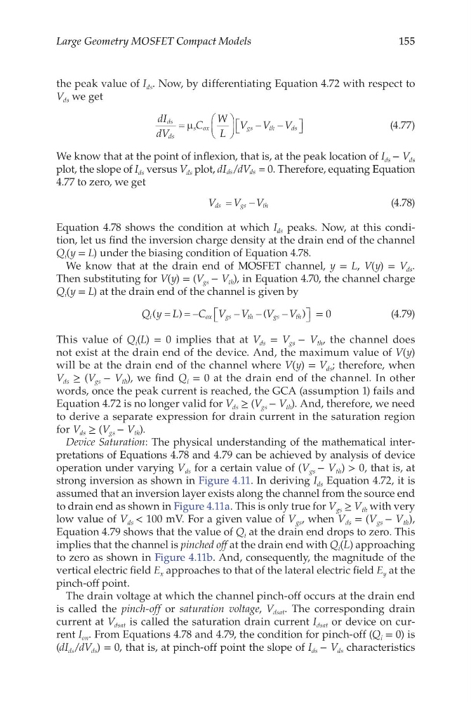
dI
dV
C
W
L
V V V
ds
ds
s ox
g s
t h
d s
=
−
−
µ
(4.77)
We know that at the point of inflexion, that is, at the peak location of I ds − V ds
plot, the slope of I ds versus V ds plot, dI dV
ds
ds
/
= 0. Therefore, equating Equation
4.77 to zero, we get
V
V V
ds
gs
t h
=
−
(4.78)
Equation 4.78 shows the condition at which I ds peaks. Now, at this condition, let us find the inversion charge density at the drain end of the channel
Q i (y = L) under the biasing condition of Equation 4.78.
We know that at the drain end of MOSFET channel, y = L, V(y) = V ds .
Then substituting for V(y) = (V gs − V th ), in Equation 4.70, the channel charge
Q i (y = L) at the drain end of the channel is given by
Q y L
C V V
V V
i
o x
g s
t h
g s
t h
(
)
(
)
= = −
−
−
−
= 0
(4.79)
This value of Q i (L) = 0 implies that at V ds = V gs − V th , the channel does
not exist at the drain end of the device. And, the maximum value of V(y)
will be at the drain end of the channel where V(y) = V ds ; therefore, when
V ds ≥ (V gs − V th ), we find Q i = 0 at the drain end of the channel. In other
words, once the peak current is reached, the GCA (assumption 1) fails and
Equation 4.72 is no longer valid for V ds ≥ (V gs − V th ). And, therefore, we need
to derive a separate expression for drain current in the saturation region
for V ds ≥ (V gs − V th ).
Device Saturation: The physical understanding of the mathematical interpretations of Equations 4.78 and 4.79 can be achieved by analysis of device
operation under varying V ds for a certain value of (V gs − V th ) > 0, that is, at
strong inversion as shown in Figure 4.11. In deriving I ds Equation 4.72, it is
assumed that an inversion layer exists along the channel from the source end
to drain end as shown in Figure 4.11a. This is only true for V gs ≥ V th with very
low value of V ds < 100 mV. For a given value of V gs , when V ds = (V gs − V th ),
Equation 4.79 shows that the value of Q i at the drain end drops to zero. This
implies that the channel is pinched off at the drain end with Q i (L) approaching
to zero as shown in Figure 4.11b. And, consequently, the magnitude of the
vertical electric field E x approaches to that of the lateral electric field E y at the
pinch-off point.
The drain voltage at which the channel pinch-off occurs at the drain end
is called the pinch-off or saturation voltage, V dsat . The corresponding drain
current at V dsat is called the saturation drain current I dsat or device on current I on . From Equations 4.78 and 4.79, the condition for pinch-off (Q i = 0) is
(dI ds /dV ds ) = 0, that is, at pinch-off point the slope of I ds − V ds characteristics
Large Geometry MOSFET Compact Models
the peak value of I ds . Now, by differentiating Equation 4.72 with respect to
V ds we get
dI
dV
C
W
L
V V V
ds
ds
s ox
g s
t h
d s
=
−
−
µ
(4.77)
We know that at the point of inflexion, that is, at the peak location of I ds − V ds
plot, the slope of I ds versus V ds plot, dI dV
ds
ds
/
= 0. Therefore, equating Equation
4.77 to zero, we get
V
V V
ds
gs
t h
=
−
(4.78)
Equation 4.78 shows the condition at which I ds peaks. Now, at this condition, let us find the inversion charge density at the drain end of the channel
Q i (y = L) under the biasing condition of Equation 4.78.
We know that at the drain end of MOSFET channel, y = L, V(y) = V ds .
Then substituting for V(y) = (V gs − V th ), in Equation 4.70, the channel charge
Q i (y = L) at the drain end of the channel is given by
Q y L
C V V
V V
i
o x
g s
t h
g s
t h
(
)
(
)
= = −
−
−
−
= 0
(4.79)
This value of Q i (L) = 0 implies that at V ds = V gs − V th , the channel does
not exist at the drain end of the device. And, the maximum value of V(y)
will be at the drain end of the channel where V(y) = V ds ; therefore, when
V ds ≥ (V gs − V th ), we find Q i = 0 at the drain end of the channel. In other
words, once the peak current is reached, the GCA (assumption 1) fails and
Equation 4.72 is no longer valid for V ds ≥ (V gs − V th ). And, therefore, we need
to derive a separate expression for drain current in the saturation region
for V ds ≥ (V gs − V th ).
Device Saturation: The physical understanding of the mathematical interpretations of Equations 4.78 and 4.79 can be achieved by analysis of device
operation under varying V ds for a certain value of (V gs − V th ) > 0, that is, at
strong inversion as shown in Figure 4.11. In deriving I ds Equation 4.72, it is
assumed that an inversion layer exists along the channel from the source end
to drain end as shown in Figure 4.11a. This is only true for V gs ≥ V th with very
low value of V ds < 100 mV. For a given value of V gs , when V ds = (V gs − V th ),
Equation 4.79 shows that the value of Q i at the drain end drops to zero. This
implies that the channel is pinched off at the drain end with Q i (L) approaching
to zero as shown in Figure 4.11b. And, consequently, the magnitude of the
vertical electric field E x approaches to that of the lateral electric field E y at the
pinch-off point.
The drain voltage at which the channel pinch-off occurs at the drain end
is called the pinch-off or saturation voltage, V dsat . The corresponding drain
current at V dsat is called the saturation drain current I dsat or device on current I on . From Equations 4.78 and 4.79, the condition for pinch-off (Q i = 0) is
(dI ds /dV ds ) = 0, that is, at pinch-off point the slope of I ds − V ds characteristics