

148
Compact Models for Integrated Circuit Design
I
C
W
L
V V
ds
s ox
g b
f b
s L
s
sL
s
s L
s
1
0
2
0
2
3 2
0
1
2
2
3
=
−
(
) −
(
)−
−
(
) −
−
µ
φ
φ
φ
φ
γ φ
φ
/
3 3 2
/
(
)
(4.48)
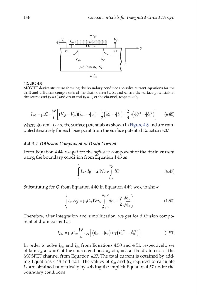
where, f s0 and f sL are the surface potentials as shown in Figure 4.8 and are computed iteratively for each bias point from the surface potential Equation 4.37.
4.4.3.2 Diffusion Component of Drain Current
From Equation 4.44, we get for the diffusion component of the drain current
using the boundary condition from Equation 4.46 as
I dy
Wv
dQ
ds
L
s
k T
i
s
sL
2
0
0
∫
∫
= µ
φ
φ
(4.49)
Substituting for Q i from Equation 4.40 in Equation 4.49, we can show
I dy
C Wv
d
d
ds
L
s ox
k T
s
s
s
s
sL
2
0
2
0
∫
∫
=
+
µ
φ
γ φ
φ
φ
φ
(4.50)
Therefore, after integration and simplification, we get for diffusion component of drain current as
I
C
W
L
v
ds
s ox
k T
s L
s
sL
s
2
0
1 2
0
1 2
=
−
(
)+
−
(
)
µ
φ
φ
γ φ
φ
/
/
(4.51)
In order to solve I ds1 and I ds2 from Equations 4.50 and 4.51, respectively, we
obtain f s0 at y = 0 at the source end and f sL at y = L at the drain end of the
MOSFET channel from Equation 4.37. The total current is obtained by adding Equations 4.48 and 4.51. The values of f s0 and f sL required to calculate
I ds are obtained numerically by solving the implicit Equation 4.37 under the
boundary conditions
V bs
p-Substrate, N b
n+
n+
V ds
V gs
Gate
T ox
V s
Oxide
ϕ s0
ϕ sL
x
y
FIGURE 4.8
MOSFET device structure showing the boundary conditions to solve current equations for the
drift and diffusion components of the drain currents; f s0 and f sL are the surface potentials at
the source end (y = 0) and drain end (y = L) of the channel, respectively.
Compact Models for Integrated Circuit Design
I
C
W
L
V V
ds
s ox
g b
f b
s L
s
sL
s
s L
s
1
0
2
0
2
3 2
0
1
2
2
3
=
−
(
) −
(
)−
−
(
) −
−
µ
φ
φ
φ
φ
γ φ
φ
/
3 3 2
/
(
)
(4.48)
where, f s0 and f sL are the surface potentials as shown in Figure 4.8 and are computed iteratively for each bias point from the surface potential Equation 4.37.
4.4.3.2 Diffusion Component of Drain Current
From Equation 4.44, we get for the diffusion component of the drain current
using the boundary condition from Equation 4.46 as
I dy
Wv
dQ
ds
L
s
k T
i
s
sL
2
0
0
∫
∫
= µ
φ
φ
(4.49)
Substituting for Q i from Equation 4.40 in Equation 4.49, we can show
I dy
C Wv
d
d
ds
L
s ox
k T
s
s
s
s
sL
2
0
2
0
∫
∫
=
+
µ
φ
γ φ
φ
φ
φ
(4.50)
Therefore, after integration and simplification, we get for diffusion component of drain current as
I
C
W
L
v
ds
s ox
k T
s L
s
sL
s
2
0
1 2
0
1 2
=
−
(
)+
−
(
)
µ
φ
φ
γ φ
φ
/
/
(4.51)
In order to solve I ds1 and I ds2 from Equations 4.50 and 4.51, respectively, we
obtain f s0 at y = 0 at the source end and f sL at y = L at the drain end of the
MOSFET channel from Equation 4.37. The total current is obtained by adding Equations 4.48 and 4.51. The values of f s0 and f sL required to calculate
I ds are obtained numerically by solving the implicit Equation 4.37 under the
boundary conditions
V bs
p-Substrate, N b
n+
n+
V ds
V gs
Gate
T ox
V s
Oxide
ϕ s0
ϕ sL
x
y
FIGURE 4.8
MOSFET device structure showing the boundary conditions to solve current equations for the
drift and diffusion components of the drain currents; f s0 and f sL are the surface potentials at
the source end (y = 0) and drain end (y = L) of the channel, respectively.