

134
Compact Models for Integrated Circuit Design
with impurities same as the well type, (3) halo implants with impurities same
as the well type, and (4) source-drain (S/D) engineering to implant S/D with
impurities opposite to the well-type. The channel engineering with V th adjust
implant produces vertically nonuniform channel doping profile and S/D
engineering with halo implants produces laterally nonuniform channel doping profile in advanced bulk MOSFET devices [7–11].
A MOSFET structure shown in Figures 4.1 and 4.2 can be characterized
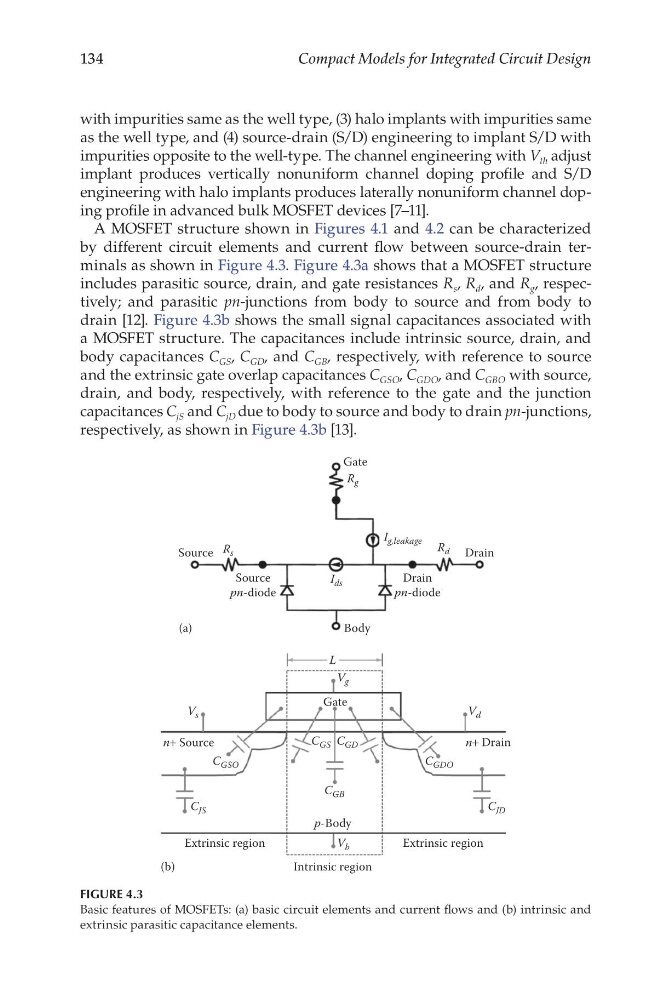
by different circuit elements and current flow between source-drain terminals as shown in Figure 4.3. Figure 4.3a shows that a MOSFET structure
includes parasitic source, drain, and gate resistances R s , R d , and R g , respectively; and parasitic pn-junctions from body to source and from body to
drain [12]. Figure 4.3b shows the small signal capacitances associated with
a MOSFET structure. The capacitances include intrinsic source, drain, and
body capacitances C GS , C GD , and C GB , respectively, with reference to source
and the extrinsic gate overlap capacitances C GSO , C GDO , and C GBO with source,
drain, and body, respectively, with reference to the gate and the junction
capacitances C jS and C jD due to body to source and body to drain pn- junctions,
respectively, as shown in Figure 4.3b [13].
Source
pn-diode
Body
(a)
Drain
pn-diode
Drain
R d
R g
Gate
I g,leakage
Source R s
I ds
L
Gate
n+ Source
n+ Drain
V g
V s
C GSO
C GB
C GS C GD
C GDO
C JS
C JD
V b
Extrinsic region
Extrinsic region
Intrinsic region
(b)
p-Body
V d
FIGURE 4.3
Basic features of MOSFETs: (a) basic circuit elements and current flows and (b) intrinsic and
extrinsic parasitic capacitance elements.
Compact Models for Integrated Circuit Design
with impurities same as the well type, (3) halo implants with impurities same
as the well type, and (4) source-drain (S/D) engineering to implant S/D with
impurities opposite to the well-type. The channel engineering with V th adjust
implant produces vertically nonuniform channel doping profile and S/D
engineering with halo implants produces laterally nonuniform channel doping profile in advanced bulk MOSFET devices [7–11].
A MOSFET structure shown in Figures 4.1 and 4.2 can be characterized
by different circuit elements and current flow between source-drain terminals as shown in Figure 4.3. Figure 4.3a shows that a MOSFET structure
includes parasitic source, drain, and gate resistances R s , R d , and R g , respectively; and parasitic pn-junctions from body to source and from body to
drain [12]. Figure 4.3b shows the small signal capacitances associated with
a MOSFET structure. The capacitances include intrinsic source, drain, and
body capacitances C GS , C GD , and C GB , respectively, with reference to source
and the extrinsic gate overlap capacitances C GSO , C GDO , and C GBO with source,
drain, and body, respectively, with reference to the gate and the junction
capacitances C jS and C jD due to body to source and body to drain pn- junctions,
respectively, as shown in Figure 4.3b [13].
Source
pn-diode
Body
(a)
Drain
pn-diode
Drain
R d
R g
Gate
I g,leakage
Source R s
I ds
L
Gate
n+ Source
n+ Drain
V g
V s
C GSO
C GB
C GS C GD
C GDO
C JS
C JD
V b
Extrinsic region
Extrinsic region
Intrinsic region
(b)
p-Body
V d
FIGURE 4.3
Basic features of MOSFETs: (a) basic circuit elements and current flows and (b) intrinsic and
extrinsic parasitic capacitance elements.