

133
Large Geometry MOSFET Compact Models
4.2.1 Basic Features of MOSFET Devices
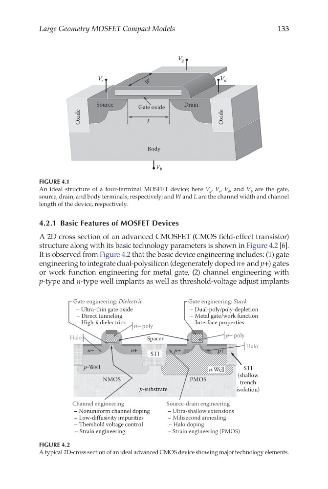
A 2D cross section of an advanced CMOSFET (CMOS field-effect transistor)
structure along with its basic technology parameters is shown in Figure 4.2 [6].
It is observed from Figure 4.2 that the basic device engineering includes: (1) gate
engineering to integrate dual-polysilicon (degenerately doped n+ and p+) gates
or work function engineering for metal gate, (2) channel engineering with
p-type and n-type well implants as well as threshold-voltage adjust implants
Body
V b
V d
V g
V s
W
Source
Drain
Gate oxide
Oxide
Oxide
L
FIGURE 4.1
An ideal structure of a four-terminal MOSFET device; here V g , V s , V d , and V b are the gate,
source, drain, and body terminals, respectively; and W and L are the channel width and channel
length of the device, respectively.
Gate engineering: Dielectric
Gate engineering: Stack
– Ultra-thin gate oxide
– Dual-poly/poly-depletion
– Interface properties
– Ultra-shallow extensions
– Nonuniform channel doping
– Low-diffusivity impurities
– Thershold voltage control
– Strain engineering
– Milisecond annealing
– Halo doping
– Strain engineering (PMOS)
– Metal gate/work function
n+ poly
p+ poly
Halo
Halo
p-Well
NMOS
PMOS
Source-drain engineering
Channel engineering
STI
n-Well
Spacer
STI
(shallow
trench
isolation)
p-substrate
n+
n+
p+
p+
– Direct tunneling
– High-k dielectrics
FIGURE 4.2
A typical 2D-cross section of an ideal advanced CMOS device showing major technology elements.
Large Geometry MOSFET Compact Models
4.2.1 Basic Features of MOSFET Devices
A 2D cross section of an advanced CMOSFET (CMOS field-effect transistor)
structure along with its basic technology parameters is shown in Figure 4.2 [6].
It is observed from Figure 4.2 that the basic device engineering includes: (1) gate
engineering to integrate dual-polysilicon (degenerately doped n+ and p+) gates
or work function engineering for metal gate, (2) channel engineering with
p-type and n-type well implants as well as threshold-voltage adjust implants
Body
V b
V d
V g
V s
W
Source
Drain
Gate oxide
Oxide
Oxide
L
FIGURE 4.1
An ideal structure of a four-terminal MOSFET device; here V g , V s , V d , and V b are the gate,
source, drain, and body terminals, respectively; and W and L are the channel width and channel
length of the device, respectively.
Gate engineering: Dielectric
Gate engineering: Stack
– Ultra-thin gate oxide
– Dual-poly/poly-depletion
– Interface properties
– Ultra-shallow extensions
– Nonuniform channel doping
– Low-diffusivity impurities
– Thershold voltage control
– Strain engineering
– Milisecond annealing
– Halo doping
– Strain engineering (PMOS)
– Metal gate/work function
n+ poly
p+ poly
Halo
Halo
p-Well
NMOS
PMOS
Source-drain engineering
Channel engineering
STI
n-Well
Spacer
STI
(shallow
trench
isolation)
p-substrate
n+
n+
p+
p+
– Direct tunneling
– High-k dielectrics
FIGURE 4.2
A typical 2D-cross section of an ideal advanced CMOS device showing major technology elements.