

135
Large Geometry MOSFET Compact Models
4.2.2 MOSFET Device Operation
A MOSFET device has three modes of operation such as accumulation,
depletion, and inversion similar to an MOS capacitor system. Therefore, the
theory developed for an MOS capacitor system can be directly extended to
MOSFETs by considering the channel potential due to the lateral electric
field from the source to drain terminals of the structure shown in Figure 4.1.
In conventional MOSFET device operation, the source is used as the reference
terminal with bias V s = 0 and a drain voltage V ds with reference to the source
is applied to the drain so that the S/D pn-junctions are reverse biased. Under
this biasing condition, the body or substrate current, I bs = 0, and the gate current, I gs = 0. The gate bias, V gs , controls the surface carrier densities. A certain
value of V gs , referred to as the threshold voltage (V th ), is required to create the
channel inversion layer. The parameter, V th is determined by the properties of
the structure. Thus, with reference to source potential,
• For V gs < V th , the MOSFET structure consists of two back-to-back
pn-junctions and only leakage currents (~I o of S/D pn-junctions) flow
from source to drain of the device, that is, I ds ~ 0;
• For V gs > V th , an inversion layer exists, that is, a conducting channel exists
from the drain to source of the device and a drain current I ds will flow.
The body or bulk terminal allows modulating the inversion layer from the
bottom by body bias, V bs , as well as from the top by V gs to offer more flexibility of devices at circuit operation. In normal MOSFET operation, V bs is
applied to reverse bias the source-drain pn-junctions.
4.3 MOSFET Threshold Voltage Model
All MOS capacitor equations derived in Chapter 3 are valid for large L and
large W MOSFETs with proper consideration of the lateral electric field, E y ,
due to the applied drain bias, V ds , as shown in Figure 4.4.
Let us consider the source potential V s = 0 as the reference voltage for
MOSFETs. Due to the applied V ds , the surface potential, f s , is a function of
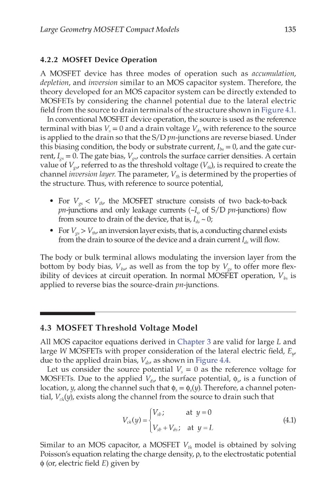
location, y, along the channel such that f s = f s (y). Therefore, a channel potential, V ch (y), exists along the channel from the source to drain such that
V y
V
y
V V
y L
ch
sb
sb
ds
( )
;
;
=
=
+
=
at
at
0
(4.1)
Similar to an MOS capacitor, a MOSFET V th model is obtained by solving
Poisson’s equation relating the charge density, ρ, to the electrostatic potential
f (or, electric field E) given by
Large Geometry MOSFET Compact Models
4.2.2 MOSFET Device Operation
A MOSFET device has three modes of operation such as accumulation,
depletion, and inversion similar to an MOS capacitor system. Therefore, the
theory developed for an MOS capacitor system can be directly extended to
MOSFETs by considering the channel potential due to the lateral electric
field from the source to drain terminals of the structure shown in Figure 4.1.
In conventional MOSFET device operation, the source is used as the reference
terminal with bias V s = 0 and a drain voltage V ds with reference to the source
is applied to the drain so that the S/D pn-junctions are reverse biased. Under
this biasing condition, the body or substrate current, I bs = 0, and the gate current, I gs = 0. The gate bias, V gs , controls the surface carrier densities. A certain
value of V gs , referred to as the threshold voltage (V th ), is required to create the
channel inversion layer. The parameter, V th is determined by the properties of
the structure. Thus, with reference to source potential,
• For V gs < V th , the MOSFET structure consists of two back-to-back
pn-junctions and only leakage currents (~I o of S/D pn-junctions) flow
from source to drain of the device, that is, I ds ~ 0;
• For V gs > V th , an inversion layer exists, that is, a conducting channel exists
from the drain to source of the device and a drain current I ds will flow.
The body or bulk terminal allows modulating the inversion layer from the
bottom by body bias, V bs , as well as from the top by V gs to offer more flexibility of devices at circuit operation. In normal MOSFET operation, V bs is
applied to reverse bias the source-drain pn-junctions.
4.3 MOSFET Threshold Voltage Model
All MOS capacitor equations derived in Chapter 3 are valid for large L and
large W MOSFETs with proper consideration of the lateral electric field, E y ,
due to the applied drain bias, V ds , as shown in Figure 4.4.
Let us consider the source potential V s = 0 as the reference voltage for
MOSFETs. Due to the applied V ds , the surface potential, f s , is a function of
location, y, along the channel such that f s = f s (y). Therefore, a channel potential, V ch (y), exists along the channel from the source to drain such that
V y
V
y
V V
y L
ch
sb
sb
ds
( )
;
;
=
=
+
=
at
at
0
(4.1)
Similar to an MOS capacitor, a MOSFET V th model is obtained by solving
Poisson’s equation relating the charge density, ρ, to the electrostatic potential
f (or, electric field E) given by