

123
Metal-Oxide-Semiconductor System
∆
∆
T
K
K
z X
ox
ox
si
d PD
=
+
(
)
,
(3.106)
where:
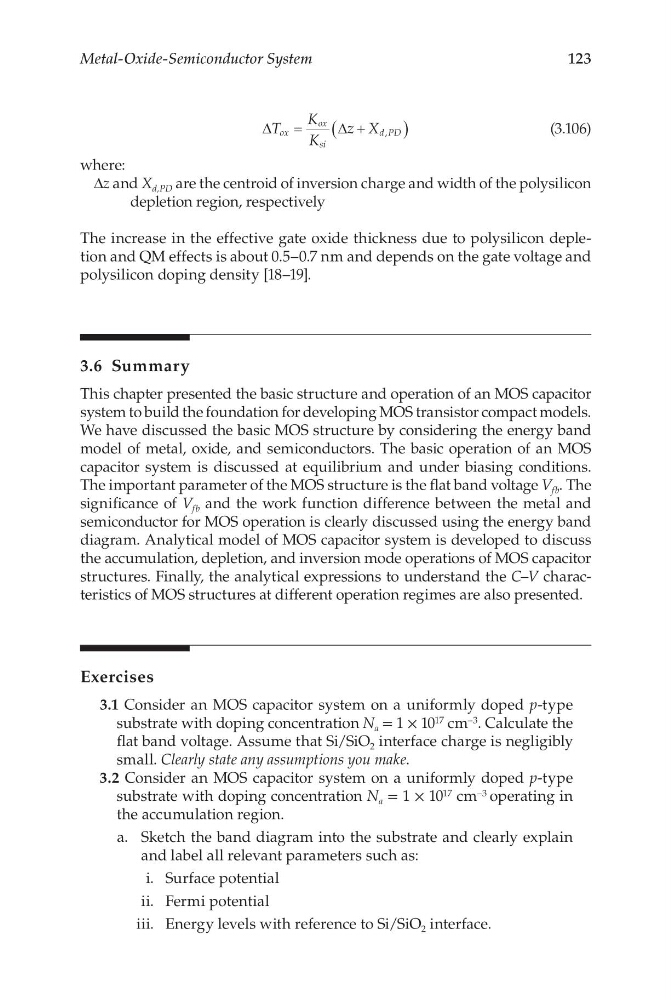
Δz and X d,PD are the centroid of inversion charge and width of the polysilicon
depletion region, respectively
The increase in the effective gate oxide thickness due to polysilicon depletion and QM effects is about 0.5–0.7 nm and depends on the gate voltage and
polysilicon doping density [18–19].
3.6 Summary
This chapter presented the basic structure and operation of an MOS capacitor
system to build the foundation for developing MOS transistor compact models.
We have discussed the basic MOS structure by considering the energy band
model of metal, oxide, and semiconductors. The basic operation of an MOS
capacitor system is discussed at equilibrium and under biasing conditions.
The important parameter of the MOS structure is the flat band voltage V fb . The
significance of V fb and the work function difference between the metal and
semiconductor for MOS operation is clearly discussed using the energy band
diagram. Analytical model of MOS capacitor system is developed to discuss
the accumulation, depletion, and inversion mode operations of MOS capacitor
structures. Finally, the analytical expressions to understand the C–V characteristics of MOS structures at different operation regimes are also presented.
Exercises
3.1 Consider an MOS capacitor system on a uniformly doped p-type
substrate with doping concentration N a = 1 × 10 17 cm –3 . Calculate the
flat band voltage. Assume that Si/SiO 2 interface charge is negligibly
small. Clearly state any assumptions you make.
3.2 Consider an MOS capacitor system on a uniformly doped p-type
substrate with doping concentration N a = 1 × 10 17 cm –3 operating in
the accumulation region.
a. Sketch the band diagram into the substrate and clearly explain
and label all relevant parameters such as:
i. Surface potential
ii. Fermi potential
iii. Energy levels with reference to Si/SiO 2 interface.
Metal-Oxide-Semiconductor System
∆
∆
T
K
K
z X
ox
ox
si
d PD
=
+
(
)
,
(3.106)
where:
Δz and X d,PD are the centroid of inversion charge and width of the polysilicon
depletion region, respectively
The increase in the effective gate oxide thickness due to polysilicon depletion and QM effects is about 0.5–0.7 nm and depends on the gate voltage and
polysilicon doping density [18–19].
3.6 Summary
This chapter presented the basic structure and operation of an MOS capacitor
system to build the foundation for developing MOS transistor compact models.
We have discussed the basic MOS structure by considering the energy band
model of metal, oxide, and semiconductors. The basic operation of an MOS
capacitor system is discussed at equilibrium and under biasing conditions.
The important parameter of the MOS structure is the flat band voltage V fb . The
significance of V fb and the work function difference between the metal and
semiconductor for MOS operation is clearly discussed using the energy band
diagram. Analytical model of MOS capacitor system is developed to discuss
the accumulation, depletion, and inversion mode operations of MOS capacitor
structures. Finally, the analytical expressions to understand the C–V characteristics of MOS structures at different operation regimes are also presented.
Exercises
3.1 Consider an MOS capacitor system on a uniformly doped p-type
substrate with doping concentration N a = 1 × 10 17 cm –3 . Calculate the
flat band voltage. Assume that Si/SiO 2 interface charge is negligibly
small. Clearly state any assumptions you make.
3.2 Consider an MOS capacitor system on a uniformly doped p-type
substrate with doping concentration N a = 1 × 10 17 cm –3 operating in
the accumulation region.
a. Sketch the band diagram into the substrate and clearly explain
and label all relevant parameters such as:
i. Surface potential
ii. Fermi potential
iii. Energy levels with reference to Si/SiO 2 interface.