

122
Compact Models for Integrated Circuit Design
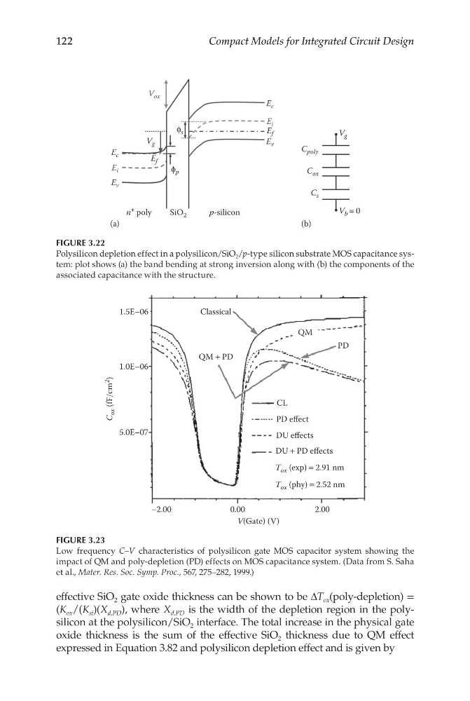
effective SiO 2 gate oxide thickness can be shown to be ΔT ox (poly-depletion) =
(K ox /(K si )(X d,PD ), where X d,PD is the width of the depletion region in the polysilicon at the polysilicon/SiO 2 interface. The total increase in the physical gate
oxide thickness is the sum of the effective SiO 2 thickness due to QM effect
expressed in Equation 3.82 and polysilicon depletion effect and is given by
−2.00
0.00
Classical
QM + PD
QM
PD
CL
PD effect
DU effects
DU + PD effects
T ox (exp) = 2.91 nm
T ox (phy) = 2.52 nm
V(Gate) (V)
5.0E–07
1.0E–06
C
ox (fF/cm
2
)
1.5E–06
2.00
FIGURE 3.23
Low frequency C–V characteristics of polysilicon gate MOS capacitor system showing the
impact of QM and poly-depletion (PD) effects on MOS capacitance system. (Data from S. Saha
et al., Mater. Res. Soc. Symp. Proc., 567, 275–282, 1999.)
SiO 2
n
+ poly
p-silicon
(a)
(b)
E v
E i
V g
E f
C poly
V g
V b = 0
C ox
C s
E f
E i
ϕ p
ϕ s
E v
E c
V ox
E c
FIGURE 3.22
Polysilicon depletion effect in a polysilicon/SiO 2 /p-type silicon substrate MOS capacitance system: plot shows (a) the band bending at strong inversion along with (b) the components of the
associated capacitance with the structure.
Compact Models for Integrated Circuit Design
effective SiO 2 gate oxide thickness can be shown to be ΔT ox (poly-depletion) =
(K ox /(K si )(X d,PD ), where X d,PD is the width of the depletion region in the polysilicon at the polysilicon/SiO 2 interface. The total increase in the physical gate
oxide thickness is the sum of the effective SiO 2 thickness due to QM effect
expressed in Equation 3.82 and polysilicon depletion effect and is given by
−2.00
0.00
Classical
QM + PD
QM
PD
CL
PD effect
DU effects
DU + PD effects
T ox (exp) = 2.91 nm
T ox (phy) = 2.52 nm
V(Gate) (V)
5.0E–07
1.0E–06
C
ox (fF/cm
2
)
1.5E–06
2.00
FIGURE 3.23
Low frequency C–V characteristics of polysilicon gate MOS capacitor system showing the
impact of QM and poly-depletion (PD) effects on MOS capacitance system. (Data from S. Saha
et al., Mater. Res. Soc. Symp. Proc., 567, 275–282, 1999.)
SiO 2
n
+ poly
p-silicon
(a)
(b)
E v
E i
V g
E f
C poly
V g
V b = 0
C ox
C s
E f
E i
ϕ p
ϕ s
E v
E c
V ox
E c
FIGURE 3.22
Polysilicon depletion effect in a polysilicon/SiO 2 /p-type silicon substrate MOS capacitance system: plot shows (a) the band bending at strong inversion along with (b) the components of the
associated capacitance with the structure.