

119
Metal-Oxide-Semiconductor System
However, if the frequency of the AC voltage signal is too high (typically,
above 1 × 10 5 Hz), the inversion charge cannot respond to the changes in AC
voltage. As a result, the measured C–V curve, called the high frequency (HF)
C–V plot is significantly different from the LF C–V plot. Also, we derived
Equation 3.87 assuming that all charges in the depletion region of an MOS
capacitor follow the variation of f s . Thus, Equation 3.87 is valid for LF C–V
curve. On the other hand, the HF capacitance of an MOS system can be
obtained by considering only the depletion charge, Q b , at the surface and
the effective depth, X d , of the depletion region at inversion condition using
parallel plate capacitance formula, C K
X
si
d
= ε 0 / .
In the accumulation and depletion regions of an MOS capacitor system, the
minority carrier charge is negligibly small compared to the bulk charge and
the total charge at the surface is primarily due to the majority carriers. As a
result, MOS capacitance in these regions is independent of frequency at all
range of operational frequency.
3.5.2 Intermediate and High Frequency C–V Characteristics
We discussed in the previous section that there are plenty of majority carriers in the substrate that can respond to the AC signal. However, the minority
carriers are scarce and have to originate by diffusion from the bulk substrate,
by generation in the depletion region, or by external sources (e.g., n+ diffusion region in MOS transistors). Thus, the inversion charge cannot respond
to the applied AC signal higher than 100 Hz. Therefore, at any HF-applied
signal to V g , the inversion charge Q i is assumed to be a constant, and therefore Q b = Q s . Thus, at any HF-applied signal to V g , only Q b will vary with the
signal around its maximum value Q bmax , and X d will vary with the signal
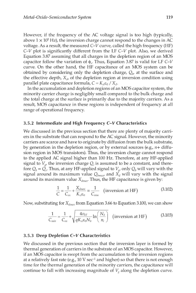
around its maximum value X dmax . Thus, the HF capacitance is given by:
1
1
1
0
C C
X
K
C
ox
dmax
si
min
=
+
≡
(
)
ε
inversion at HF
(3.102)
Now, substituting for X dmax from Equation 3.66 to Equation 3.100, we can show
1
1
4
0
C
C
v
qK N
N
n
min
ox
kT
si
b
b
i
=
+
(
)
ε
ln
inversion at HF
(3.103)
3.5.3 Deep Depletion C–V Characteristics
We discussed in the previous section that the inversion layer is formed by
thermal generation of carriers in the substrate of an MOS capacitor. However,
if an MOS capacitor is swept from the accumulation to the inversion regions
at a relatively fast rate (e.g., 10 V sec –1 and higher) so that there is not enough
time for the thermal generation of the minority carriers, the capacitance will
continue to fall with increasing magnitude of V g along the depletion curve.
Metal-Oxide-Semiconductor System
However, if the frequency of the AC voltage signal is too high (typically,
above 1 × 10 5 Hz), the inversion charge cannot respond to the changes in AC
voltage. As a result, the measured C–V curve, called the high frequency (HF)
C–V plot is significantly different from the LF C–V plot. Also, we derived
Equation 3.87 assuming that all charges in the depletion region of an MOS
capacitor follow the variation of f s . Thus, Equation 3.87 is valid for LF C–V
curve. On the other hand, the HF capacitance of an MOS system can be
obtained by considering only the depletion charge, Q b , at the surface and
the effective depth, X d , of the depletion region at inversion condition using
parallel plate capacitance formula, C K
X
si
d
= ε 0 / .
In the accumulation and depletion regions of an MOS capacitor system, the
minority carrier charge is negligibly small compared to the bulk charge and
the total charge at the surface is primarily due to the majority carriers. As a
result, MOS capacitance in these regions is independent of frequency at all
range of operational frequency.
3.5.2 Intermediate and High Frequency C–V Characteristics
We discussed in the previous section that there are plenty of majority carriers in the substrate that can respond to the AC signal. However, the minority
carriers are scarce and have to originate by diffusion from the bulk substrate,
by generation in the depletion region, or by external sources (e.g., n+ diffusion region in MOS transistors). Thus, the inversion charge cannot respond
to the applied AC signal higher than 100 Hz. Therefore, at any HF-applied
signal to V g , the inversion charge Q i is assumed to be a constant, and therefore Q b = Q s . Thus, at any HF-applied signal to V g , only Q b will vary with the
signal around its maximum value Q bmax , and X d will vary with the signal
around its maximum value X dmax . Thus, the HF capacitance is given by:
1
1
1
0
C C
X
K
C
ox
dmax
si
min
=
+
≡
(
)
ε
inversion at HF
(3.102)
Now, substituting for X dmax from Equation 3.66 to Equation 3.100, we can show
1
1
4
0
C
C
v
qK N
N
n
min
ox
kT
si
b
b
i
=
+
(
)
ε
ln
inversion at HF
(3.103)
3.5.3 Deep Depletion C–V Characteristics
We discussed in the previous section that the inversion layer is formed by
thermal generation of carriers in the substrate of an MOS capacitor. However,
if an MOS capacitor is swept from the accumulation to the inversion regions
at a relatively fast rate (e.g., 10 V sec –1 and higher) so that there is not enough
time for the thermal generation of the minority carriers, the capacitance will
continue to fall with increasing magnitude of V g along the depletion curve.