

118
Compact Models for Integrated Circuit Design
Q
qK N
C
qK N
C
qK N V V
b
si
b
ox
si
b
ox
si
b
g
fb
=
±
+
−
(
)
ε
ε
ε
0
0
2
0
2
(3.97)
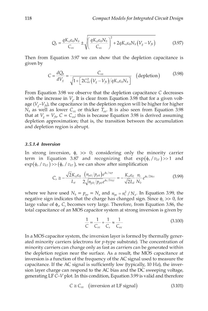
Then from Equation 3.97 we can show that the depletion capacitance is
given by
C
dQ
dV
C
C V V qK N
b
g
ox
ox
g
f b
s i
b
=
=
+
−
(
)
(
)
1 2
2
0
ε
depletion
(3.98)
From Equation 3.98 we observe that the depletion capacitance C decreases
with the increase in V g . It is clear from Equation 3.98 that for a given voltage (V g –V fb ), the capacitance in the depletion region will be higher for higher
N b as well as lower C ox or thicker T ox . It is also seen from Equation 3.98
that at V g = V fb , C = C ox ; this is because Equation 3.98 is derived assuming
depletion approximation; that is, the transition between the accumulation
and depletion region is abrupt.
3.5.1.4 Inversion
In strong inversion, f s >> 0; considering only the minority carrier
term in Equation 3.87 and recognizing that exp /
φ s k T
v
(
)>> 1 and
exp /
/
φ
φ
s
k T
s
kT
v
v
(
)>> (
), we can show after simplification
C
K
L
n p e
n p e
K
L
n
N
e
s
si
d
p
p
v
p
p
v
si
d
i
b
s kT
s
k T
s
≅ −
(
)
= −
2
2
2
0
0
0
0
0
2
0
2
ε
ε
φ
φ
φ v vkT
(3.99)
where we have used N b = p po = N a and n
n N
p
i
a
o =
2 / . In Equation 3.99, the
negative sign indicates that the charge has changed sign. Since f s >> 0, for
large value of f s , C s becomes very large. Therefore, from Equation 3.86, the
total capacitance of an MOS capacitor system at strong inversion is given by
1
1
1
1
C C
C
C
ox
s
o x
=
+
≈
(3.100)
In a MOS capacitor system, the inversion layer is formed by thermally generated minority carriers (electrons for p-type substrate). The concentration of
minority carriers can change only as fast as carriers can be generated within
the depletion region near the surface. As a result, the MOS capacitance at
inversion is a function of the frequency of the AC signal used to measure the
capacitance. If the AC signal is sufficiently low (typically, 10 Hz), the inversion layer charge can respond to the AC bias and the DC sweeping voltage,
generating LF C–V plot. In this condition, Equation 3.99 is valid and therefore
C C ox
≅
(
)
inversion at LF signal
(3.101)
Compact Models for Integrated Circuit Design
Q
qK N
C
qK N
C
qK N V V
b
si
b
ox
si
b
ox
si
b
g
fb
=
±
+
−
(
)
ε
ε
ε
0
0
2
0
2
(3.97)
Then from Equation 3.97 we can show that the depletion capacitance is
given by
C
dQ
dV
C
C V V qK N
b
g
ox
ox
g
f b
s i
b
=
=
+
−
(
)
(
)
1 2
2
0
ε
depletion
(3.98)
From Equation 3.98 we observe that the depletion capacitance C decreases
with the increase in V g . It is clear from Equation 3.98 that for a given voltage (V g –V fb ), the capacitance in the depletion region will be higher for higher
N b as well as lower C ox or thicker T ox . It is also seen from Equation 3.98
that at V g = V fb , C = C ox ; this is because Equation 3.98 is derived assuming
depletion approximation; that is, the transition between the accumulation
and depletion region is abrupt.
3.5.1.4 Inversion
In strong inversion, f s >> 0; considering only the minority carrier
term in Equation 3.87 and recognizing that exp /
φ s k T
v
(
)>> 1 and
exp /
/
φ
φ
s
k T
s
kT
v
v
(
)>> (
), we can show after simplification
C
K
L
n p e
n p e
K
L
n
N
e
s
si
d
p
p
v
p
p
v
si
d
i
b
s kT
s
k T
s
≅ −
(
)
= −
2
2
2
0
0
0
0
0
2
0
2
ε
ε
φ
φ
φ v vkT
(3.99)
where we have used N b = p po = N a and n
n N
p
i
a
o =
2 / . In Equation 3.99, the
negative sign indicates that the charge has changed sign. Since f s >> 0, for
large value of f s , C s becomes very large. Therefore, from Equation 3.86, the
total capacitance of an MOS capacitor system at strong inversion is given by
1
1
1
1
C C
C
C
ox
s
o x
=
+
≈
(3.100)
In a MOS capacitor system, the inversion layer is formed by thermally generated minority carriers (electrons for p-type substrate). The concentration of
minority carriers can change only as fast as carriers can be generated within
the depletion region near the surface. As a result, the MOS capacitance at
inversion is a function of the frequency of the AC signal used to measure the
capacitance. If the AC signal is sufficiently low (typically, 10 Hz), the inversion layer charge can respond to the AC bias and the DC sweeping voltage,
generating LF C–V plot. In this condition, Equation 3.99 is valid and therefore
C C ox
≅
(
)
inversion at LF signal
(3.101)