

112
Compact Models for Integrated Circuit Design
d x
dx
qN v
K
x
v
n
N
e
a kT
si
kT
i
a
x vkT
φ
ε
φ
φ
( )
( )
( )
= −
+
2
0
2
2
(3.78)
Equation 3.78 must be solved numerically with boundary condition, f(x) = f s
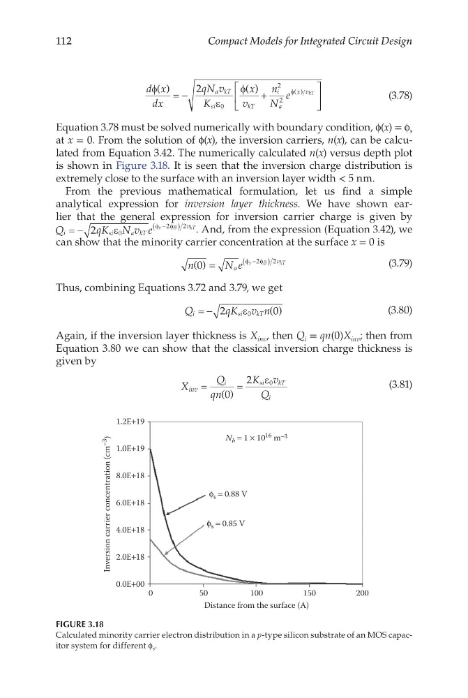
at x = 0. From the solution of f(x), the inversion carriers, n(x), can be calculated from Equation 3.42. The numerically calculated n(x) versus depth plot
is shown in Figure 3.18. It is seen that the inversion charge distribution is
extremely close to the surface with an inversion layer width < 5 nm.
From the previous mathematical formulation, let us find a simple
analytical expression for inversion layer thickness. We have shown earlier that the general expression for inversion carrier charge is given by
Q
q K N v e
i
s i
a kT
v
s
B
kT
= −
−
(
)
2
0
2
2
ε
φ
φ
. And, from the expression (Equation 3.42), we
can show that the minority carrier concentration at the surface x = 0 is
n
N e
a
v
s
B
kT
( )
0
2
2
=
−
(
)
φ
φ
(3.79)
Thus, combining Equations 3.72 and 3.79, we get
Q
q K v n
i
s i
k T
= − 2
0
0
ε
( )
(3.80)
Again, if the inversion layer thickness is X inv , then Q i = qn(0)X inv ; then from
Equation 3.80 we can show that the classical inversion charge thickness is
given by
X
Q
qn
K v
Q
inv
i
s i
k T
i
=
=
( )
0
2
0
ε
(3.81)
0
0.0E+00
2.0E+18
4.0E+18
6.0E+18
8.0E+18
1.0E+19
1.2E+19
Inversion carrier concentration (cm
–3
)
50
ϕ s = 0.85 V
ϕ s = 0.88 V
N b = 1 × 10
16 m −3
100
Distance from the surface (A)
150
200
FIGURE 3.18
Calculated minority carrier electron distribution in a p-type silicon substrate of an MOS capacitor system for different f s .
Compact Models for Integrated Circuit Design
d x
dx
qN v
K
x
v
n
N
e
a kT
si
kT
i
a
x vkT
φ
ε
φ
φ
( )
( )
( )
= −
+
2
0
2
2
(3.78)
Equation 3.78 must be solved numerically with boundary condition, f(x) = f s
at x = 0. From the solution of f(x), the inversion carriers, n(x), can be calculated from Equation 3.42. The numerically calculated n(x) versus depth plot
is shown in Figure 3.18. It is seen that the inversion charge distribution is
extremely close to the surface with an inversion layer width < 5 nm.
From the previous mathematical formulation, let us find a simple
analytical expression for inversion layer thickness. We have shown earlier that the general expression for inversion carrier charge is given by
Q
q K N v e
i
s i
a kT
v
s
B
kT
= −
−
(
)
2
0
2
2
ε
φ
φ
. And, from the expression (Equation 3.42), we
can show that the minority carrier concentration at the surface x = 0 is
n
N e
a
v
s
B
kT
( )
0
2
2
=
−
(
)
φ
φ
(3.79)
Thus, combining Equations 3.72 and 3.79, we get
Q
q K v n
i
s i
k T
= − 2
0
0
ε
( )
(3.80)
Again, if the inversion layer thickness is X inv , then Q i = qn(0)X inv ; then from
Equation 3.80 we can show that the classical inversion charge thickness is
given by
X
Q
qn
K v
Q
inv
i
s i
k T
i
=
=
( )
0
2
0
ε
(3.81)
0
0.0E+00
2.0E+18
4.0E+18
6.0E+18
8.0E+18
1.0E+19
1.2E+19
Inversion carrier concentration (cm
–3
)
50
ϕ s = 0.85 V
ϕ s = 0.88 V
N b = 1 × 10
16 m −3
100
Distance from the surface (A)
150
200
FIGURE 3.18
Calculated minority carrier electron distribution in a p-type silicon substrate of an MOS capacitor system for different f s .